
Page 429 - DSP Integrated Circuits
P. 429
414 Chapter 9 Synthesis of DSP Architectures
operations in 0.32 ms using an access rate for the memories of 32 MHz. A set of
shift registers, one for each input/output of the PEs, is used as converters between
the bit-parallel and bit-serial parts. The shift registers can be viewed as cache
memories used to obtain uniform access patterns for the RAMs.
9.9.1 Selecting the Interconnection Network
In this section we will discuss the effect on the interconnection network (ICN)
resulting from different choices of RAM and PE assignments. In general, the
assignments, discussed in section 7.12, lead to four different architectures, since
we have two alternative assignments each for RAMs and PEs. We summarize the
resulting architectures next. Detailed derivation of the architectures is left as an
exercise.
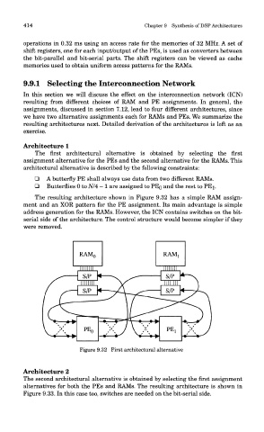
Architecture 1
The first architectural alternative is obtained by selecting the first
assignment alternative for the PEs and the second alternative for the RAMs. This
architectural alternative is described by the following constraints:
Q A butterfly PE shall always use data from two different RAMs.
Q Butterflies 0 to N/4 - I are assigned to PEo and the rest to PEi.
The resulting architecture shown in Figure 9.32 has a simple RAM assign-
ment and an XOR pattern for the PE assignment. Its main advantage is simple
address generation for the RAMs. However, the ICN contains switches on the bit-
serial side of the architecture. The control structure would become simpler if they
were removed.
Figure 9.32 First architectural alternative
Architecture 2
The second architectural alternative is obtained by selecting the first assignment
alternatives for both the PEs and RAMs. The resulting architecture is shown in
Figure 9.33. In this case too, switches are needed on the bit-serial side.