
Page 432 - DSP Integrated Circuits
P. 432
9.9 FFT Processor, Cont. 417
ory. The goal of this section is to find which function these processes must have to get
the desired address sequences for the RAMs. We will describe the control and address
generation for the third architectural alternative only. This architecture does not have
switches on the bit-serial side, instead the ICN contains a switching function on the
bit-parallel side to select which of the registers in the S/P converters to use.
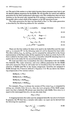
The index generation for data was described in Box 7.4. The index generation
is described by the following indices for the variables:
These are the four indices for data to be used in the butterflies and the expo-
nent, p, to compute WP. In the following index kl will be denoted the base index.
The other indices, k-tff ,k%, and &22V can De computed by setting bits in the binary
representation of the base index. In the equation for k% there is a term N s/2 or 2N S
that is added to the base index. This term is hereafter called BF, denoting that it is
used to derive the index for the second butterfly process.
We must now find a way to transform this into a description with two RAMs,
two butterfly PEs, cache memories, and some address generation for the RAMs
and cache memories. First we will study how to transform from the indices to the
selection of RAMs and PEs in the chosen assignment. Variables are assigned to
RAMs through the P function denned in Equation (7.8). We can derive the follow-
ing assignments of the various indices:
For example, P(ku\f s) is always the inverse of P(ki) since &L/VS is computed by
setting one, initially reset, bit in k\. Also, the main property of this RAM assign-
ment was that a butterfly PE always uses data from both RAMs. Now, since k\ is
equal to the rearranged bits of m, we can also state that
A mapping between the index and the assigned butterfly has also to be found.
In general, the PE that has a variable with index i as input can be derived from
the following two equations: