
Page 434 - DSP Integrated Circuits
P. 434
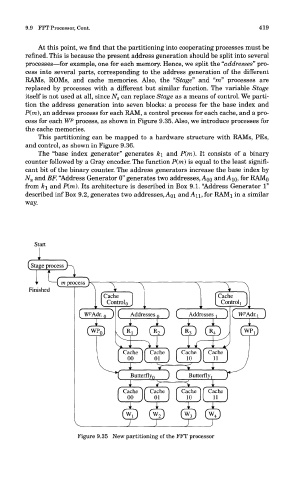
9.9 FFT Processor, Cont.                                              419

            At this point, we find that the partitioning into cooperating processes must be
        refined. This is because the present address generation should be split into several
        processes—for example, one for each memory. Hence, we split the "addresses" pro-
        cess into several parts, corresponding to the address generation of the different
        RAMs, ROMs, and cache memories. Also, the "Stage" and "m" processes are
        replaced by processes with a different but similar function. The variable Stage
        itself is not used at all, since N s can replace Stage as a means of control. We parti-
        tion the address generation into seven blocks: a process for the base index and
        P(m), an address process for each RAM, a control process for each cache, and a pro-
                      p
        cess for each W  process, as shown in Figure 9.35. Also, we introduce processes for
        the cache memories.
            This partitioning can be mapped to a hardware structure with RAMs, PEs,
        and control, as shown in Figure 9.36.
            The "base index generator" generates k\ and P(m). It consists of a binary
        counter followed by a Gray encoder. The function P(m) is equal to the least signifi-
        cant bit of the binary counter. The address generators increase the base index by
        N s and BF. "Address Generator 0" generates two addresses, AOO and AIQ, for RAMo
        from k\ and P(m). Its architecture is described in Box 9.1. "Address Generator 1"
        described inf Box 9.2, generates two addresses, AQI and AH, for RAMj in a similar
        way.


                        Figure 9.35 New partitioning of the FFT processor