
Page 435 - DSP Integrated Circuits
P. 435
420 Chapter 9 Synthesis of DSP Architectures
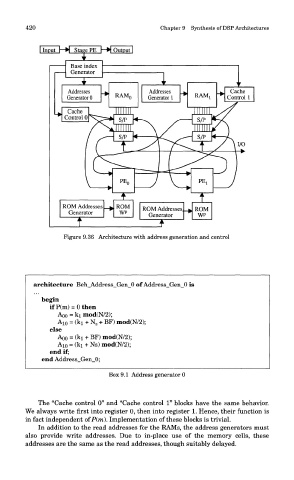
Figure 9.36 Architecture with address generation and control
architecture Beh_Address_Gen_0 of Address_Gen_0 is
begin
ifP(m) = Othen
AQO = ki mod(N/2);
AIO = (ki + N s + BF) mod(N/2);
else
AQO = (ki + BF) mod(N/2);
AIO = (ki + Ns) mod(N/2);
end if;
end Address_Gen_0;
Box 9.1 Address generator 0
The "Cache control 0" and "Cache control 1" blocks have the same behavior.
We always write first into register 0, then into register 1. Hence, their function is
in fact independent of P(m). Implementation of these blocks is trivial.
In addition to the read addresses for the RAMs, the address generators must
also provide write addresses. Due to in-place use of the memory cells, these
addresses are the same as the read addresses, though suitably delayed.