
Page 436 - DSP Integrated Circuits
P. 436
9.9 FFT Processor, Cont. 421
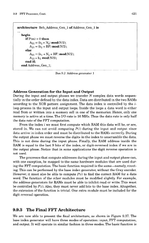
architecture Beh_Address_Gen_l of Address_Gen_l is
begin
if P(m) = 0 then
AQI = (ki + N B) mod(N/2);
An = (ki + BF) mod(N/2);
else
AQI = (ki + N s + BF) mod(N/2);
AH = ki mod(N/2);
end if;
end Address_Gen_l;
Box 9.2 Address generator 1
Address Generation for the Input and Output
During the input and output phases we transfer N complex data words sequen-
tially in the order denned by the data index. Data are distributed in the two RAMs
according to the XOR pattern assignment. The data index is controlled by the i-
loop process in the input and output loops. Inside the loops a data word is either
read from or written into a memory cell in one of the memories. Hence, only one
memory is active at a time. The I/O rate is 16 MHz. Thus the data rate is only half
the data rate of the FFT computation.
From the index i we must first compute which RAM this data will be, or are,
stored in. We can not avoid computing P(i) during the input and output since
data arrive in index order and must be distributed to the RAMs correctly. During
the output phase we must reverse the digits in the index to unscramble the data.
This is not done during the input phase. Finally, the RAM address inside the
RAM is equal to the last 9 bits of the index, or digit-reversed index if we are in
the output phase. Notice that in some applications the digit reverse operation is
not used.
The processes that compute addresses during the input and output phase can,
with one exception, be mapped to the same hardware modules that are used dur-
ing the FFT computation. The basic function required is the same—namely, count-
ing. This can be performed by the base index generator, without the Gray encoder.
However, it must also be able to compute P(i) to find the correct RAM for a data
word. The function of the other modules must be modified slightly. For example,
the address generators for RAMs must be able to inhibit read or write. This must
be controlled by P(i). Also, they must never add bits to the base index. Altogether,
the extension of the function is trivial. One extra module must be included for the
digit reversal operation.
9.9.3 The Final FFT Architecture
We are now able to present the final architecture, as shown in Figure 9.37. The
base index generator will have three modes of operation: input, FFT computation,
and output. It will operate in similar fashion in three modes. The basic function is