
Page 441 - DSP Integrated Circuits
P. 441
426 Chapter9 Synthesis of DSP Architectures
The inputs should arrive at the PEs synchronously, but the memory delivers the
values sequentially. Hence, the first delivered values must be delayed in order to
arrive at the PE at the same time as the last value delivered by the memory. Shim-
ming delays have therefore been inserted on both sides of the serial/parallel con-
verters, as shown in Figure 9.38.
To avoid access conflicts the intermediate
array must be stored in the memories prop-
erly. Further, transposition of the intermediate
array can be obtained free by storing the
array, as illustrated in Figure 9.39 [26, 27].
In the first computational phase, the PE
delivers eight values to each RAM correspond-
ing to one row in the intermediate array. In Figure 9.39 Storage of
the second phase, values corresponding to col- intermediate array in
umns should be accessed. This scheme could RAM! and RAM 2
be implemented by putting a multiplexer after
the PEs, but can be accomplished more easily by exploring the symmetry of the
basis function.
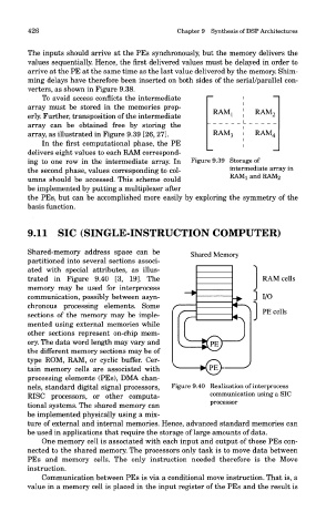
9.11 SIC (SINGLE-INSTRUCTION COMPUTER)
Shared-memory address space can be Shared Memory
partitioned into several sections associ- i •>
ated with special attributes, as illus-
trated in Figure 9.40 [3, 19]. The RAM cells
memory may be used for interprocess
communication, possibly between asyn- ~* -+ ] I/O
chronous processing elements. Some
r s ^"^j PE cells
sections of the memory may be imple-
mented using external memories while
other sections represent on-chip mem-
ory. The data word length may vary and v £(PE)
the different memory sections may be of
type ROM, RAM, or cyclic buffer. Cer-
tain memory cells are associated with ^ K§)
processing elements (PEs), DMA chan-
nels, standard digital signal processors, Figure 9.40 Realization of interprocess
RISC processors, or other computa- communication using a SIC
processor
tional systems. The shared memory can
be implemented physically using a mix-
ture of external and internal memories. Hence, advanced standard memories can
be used in applications that require the storage of large amounts of data.
One memory cell is associated with each input and output of those PEs con-
nected to the shared memory. The processors only task is to move data between
PEs and memory cells. The only instruction needed therefore is the Move
instruction.
Communication between PEs is via a conditional move instruction. That is, a
value in a memory cell is placed in the input register of the PEs and the result is