Page 420 - DSP Integrated Circuits
P. 420
9.6 Shared-Memory Architectures with Bit-Serial PEs                  405

        accessed simultaneously, as illustrated in Figure 9.19. Memory has therefore to be
        assigned such that access conflicts are avoided.
            As discussed in Chapter 8, a shared-memory architecture can only accommo-
        date a few PEs, since the cycle time for the memories and the execution time for
        the processing elements are of the same order.
            The imbalance becomes even more severe for DSP algorithms, since the pro-
        cessing elements often require many input values from the memories for each
        operation. Obviously, it is not efficient to use PEs so fast that the memories
        become the bottleneck. Generally, PEs that are faster than necessary consume
        more power and chip area. An efficient way to obtain a balanced architecture is to
        increase the execution time of the PEs as much as allowed by the application
        requirements. The cost of the system can thereby be reduced.


        9.6.1 Minimizing the Cost
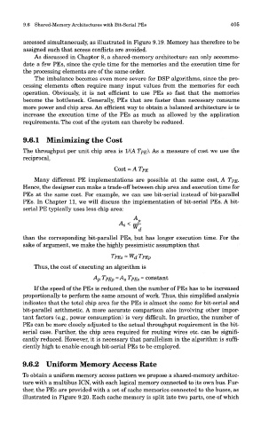
        The throughput per unit chip area is 1/(A TPE). As a measure of cost we use the
        reciprocal,


            Many different PE implementations are possible at the same cost, A TPE.
        Hence, the designer can make a trade-off between chip area and execution time for
        PEs at the same cost. For example, we can use bit-serial instead of bit-parallel
        PEs. In Chapter 11, we will discuss the implementation of bit-serial PEs. A bit-
        serial PE typically uses less chip area:


                                               ct
        than the corresponding bit-parallel PEs, but has longer execution time. For the
        sake of argument, we make the highly pessimistic assumption that


            Thus, the cost of executing an algorithm is


            If the speed of the PEs is reduced, then the number of PEs has to be increased
        proportionally to perform the same amount of work. Thus, this simplified analysis
        indicates that the total chip area for the PEs is almost the same for bit-serial and
        bit-parallel arithmetic. A more accurate comparison also involving other impor-
        tant factors (e.g., power consumption) is very difficult. In practice, the number of
        PEs can be more closely adjusted to the actual throughput requirement in the bit-
        serial case. Further, the chip area required for routing wires etc. can be signifi-
        cantly reduced. However, it is necessary that parallelism in the algorithm is suffi-
        ciently high to enable enough bit-serial PEs to be employed.

        9.6.2 Uniform Memory Access Rate

        To obtain a uniform memory access pattern we propose a shared-memory architec-
        ture with a multibus ICN, with each logical memory connected to its own bus. Fur-
        ther, the PEs are provided with a set of cache memories connected to the buses, as
        illustrated in Figure 9.20. Each cache memory is split into two parts, one of which

