
Page 503 - DSP Integrated Circuits
P. 503
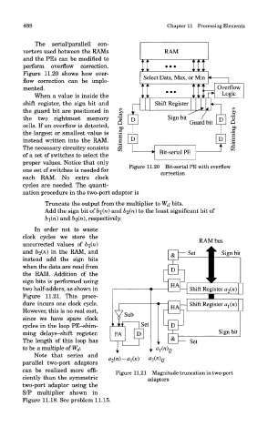
488                                           Chapter 11 Processing Elements


            The serial/parallell con-
        verters used between the RAMs
        and the PEs can be modified to
        perform overflow correction.
        Figure 11.20 shows how over-
        flow correction can be imple-
        mented.
           When a value is inside the
        shift register, the sign bit and
        the guard bit are positioned in
        the two rightmost memory
        cells. If an overflow is detected,
        the largest or smallest value is
        instead written into the RAM.
        The necessary circuitry consists
        of a set of switches to select the
        proper values. Notice that only
                                          Figure 11.20 Bit-serial PE with overflow
        one set of switches is needed for
                                                    correction
        each RAM. No extra clock
        cycles are needed. The quanti-
        zation procedure in the two-port adaptor is
               Truncate the output from the multiplier to Wj bits.
               Add the sign bit of bi(n) and b%(ri) to the least significant bit of
               &lOi) and b<z(n), respectively.
            In order not to waste
        clock cycles we store the
        uncorrected values of b\(ri)
        and b^n) in the RAM, and
        instead add the sign bits
        when the data are read from
        the RAM. Addition of the
        sign bits is performed using
        two half-adders, as shown in
        Figure 11.21. This proce-
        dure incurs one clock cycle.
        However, this is no real cost,
        since we have spare clock
        cycles in the loop PE-shim-
        ming delays—shift register.
        The length of this loop has
        to be a multiple of Wd.
           Note that series and
        parallel two-port adaptors
        can be realized more effi-
                                      Figure 11.21 Magnitude truncation in two-port
        ciently than the symmetric              adaptors
        two-port adaptor using the
        S/P multiplier shown in
        Figure 11.18. See problem 11.15.