
Page 501 - DSP Integrated Circuits
P. 501
486 Chapter 11 Processing Elements
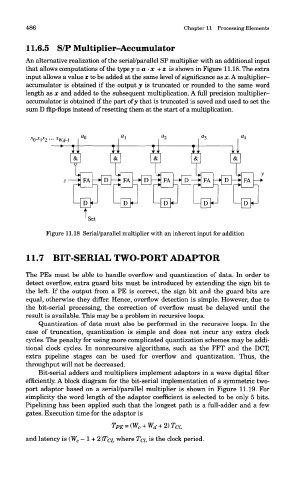
11.6.5 S/P Multiplier-Accumulator
An alternative realization of the serial/parallel SP multiplier with an additional input
that allows computations of the typey = a-x +z is shown in Figure 11.18. The extra
input allows a value z to be added at the same level of significance as x. A multiplier-
accumulator is obtained if the output y is truncated or rounded to the same word
length as x and added to the subsequent multiplication. A full precision multiplier-
accumulator is obtained if the part of y that is truncated is saved and used to set the
sum D flip-flops instead of resetting them at the start of a multiplication.
Figure 11.18 Serial/parallel multiplier with an inherent input for addition
11.7 BIT-SERIAL TWO-PORT ADAPTOR
The PEs must be able to handle overflow and quantization of data. In order to
detect overflow, extra guard bits must be introduced by extending the sign bit to
the left. If the output from a PE is correct, the sign bit and the guard bits are
equal, otherwise they differ. Hence, overflow detection is simple. However, due to
the bit-serial processing, the correction of overflow must be delayed until the
result is available. This may be a problem in recursive loops.
Quantization of data must also be performed in the recursive loops. In the
case of truncation, quantization is simple and does not incur any extra clock
cycles. The penalty for using more complicated quantization schemes may be addi-
tional clock cycles. In nonrecursive algorithms, such as the FFT and the DCT,
extra pipeline stages can be used for overflow and quantization. Thus, the
throughput will not be decreased.
Bit-serial adders and multipliers implement adaptors in a wave digital filter
efficiently. A block diagram for the bit-serial implementation of a symmetric two-
port adaptor based on a serial/parallel multiplier is shown in Figure 11.19. For
simplicity the word length of the adaptor coefficient is selected to be only 5 bits.
Pipelining has been applied such that the longest path is a full-adder and a few
gates. Execution time for the adaptor is
T PE = (W c + W d + 2)T CL
and latency is (W c -1 + 2)TcL where TCL is the clock period.