
Page 311 - Engineering Digital Design
P. 311
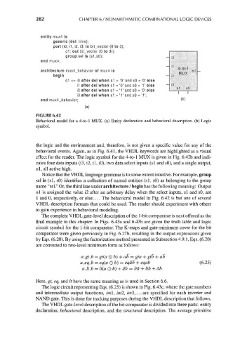
282               CHAPTER 6 / NONARITHMETIC COMBINATIONAL LOGIC DEVICES


                        entity mux4 is
                             generic (del: time);
                             port (10, i1, i2, i3: in bit_vector (0 to 3);
                                  o1: out bit_vector (0 to 3));
                                  group sel is (s1,sO);
                        end mux4;
                        architecture mux4_behavior of mux4 is
                             begin
                                  o1 <= iO after del when s1 = '0' and sO = '0' else
                                      11 after del when s1 = '0' and sO = '1' else
                                      12 after del when s1 = '1' and sO = '0' else
                                      13 after del when s1 = '1' and sO = 'V;
                        end mux4_behavior;
                                         (a)
                    FIGURE 6.42
                    Behavioral model for a 4-to-l MUX. (a) Entity declaration and behavioral description, (b) Logic
                    symbol.


                    the logic and the environment and, therefore, is not given a specific value for any of the
                    behavioral events. Again, as in Fig. 6.41, the VHDL keywords are highlighted as a visual
                    effect for the reader. The logic symbol for the 4-to-l MUX is given in Fig. 6.42b and indi-
                    cates four data inputs (i3, i2, il, iO), two data select inputs (si and sO), and a single output,
                    ol, all active high.
                      Notice that the VHDL language grammar is to some extent intuitive. For example, group
                    sel is (si, sO) identifies a collection of named entities (si, sO) as belonging to the group
                    name "sel." Or, the third line under architecture / begin has the following meaning: Output
                    ol is assigned the value i2 after an arbitrary delay when the select inputs, si and sO, are
                    1 and 0, respectively, or else  The behavioral model in Fig. 6.42 is but one of several
                    VHDL description formats that could be used. The reader should experiment with others
                    to gain experience in behavioral modeling.
                      The complete VHDL gate-level description of the 1-bit comparator is next offered as the
                    final example in this chapter. In Figs. 6.43a and 6.43b are given the truth table and logic
                    circuit symbol for the 1-bit comparator. The K-maps and gate-minimum cover for the bit
                    comparator were given previously in Fig. 6.27b, resulting in the output expressions given
                    by Eqs. (6.20). By using the factorization method presented in Subsection 4.9.1, Eqs. (6.20)
                    are converted to two-level minimum form as follows:

                                      a-gtJb = gt(a O b) + ab = gta + gtb + ab
                                      a.eqJb = eq(a O b} = eqdb + eqab                 (6.25)
                                       a JtJb = lt(a Q b) + ab = ltd + lib + db.


                    Here, gt, eq, and It have the same meaning as is used in Section 6.6.
                      The logic circuit representing Eqs. (6.25) is shown in Fig. 6.43c, where the gate numbers
                    and intermediate output functions, /ml, im2, im3,... are specified for each inverter and
                    NAND gate. This is done for tracking purposes during the VHDL description that follows.
                      The VHDL gate-level description of the bit-comparator is divided into three parts: entity
                    declaration, behavioral description, and the structural description. The average primitive