
Page 365 - Engineering Digital Design
P. 365
336 CHAPTER 8 / ARITHMETIC DEVICES AND ARITHMETIC LOGIC UNITS (ALUs)
the last three being classified as "high-speed" adders. This list of four does not nearly cover
the scope of adder design, nor does it establish the general character of these arithmetic
devices. It does introduce the concept of computational speed as it relates to the addition
process, however that is characterized.
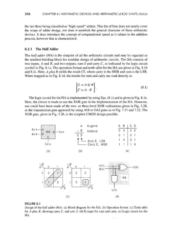
8.2.1 The Half Adder
The half adder (HA) is the simplest of all the arithmetic circuits and may be regarded as
the smallest building block for modular design of arithmetic circuits. The HA consists of
two inputs, A and B, and two outputs, sum S and carry C, as indicated by the logic circuit
symbol in Fig. 8.la. The operation format and truth table for the HA are given in Fig. 8.1b
and 8.1c. Here, A plus B yields the result CS, where carry is the MSB and sum is the LSB.
When mapped as in Fig. 8. Id, the results for sum and carry are read directly as
(8.1)
The logic circuit for the HA is implemented by using Eqs. (8.1) and is given in Fig. 8. le.
Here, the choice is made to use the XOR gate in the implementation of the HA. However,
use could have been made of the two- or three-level XOR realizations given in Fig. 3.28,
or the transmission gate approach by using AOI or OAI gates as in Fig. 7.21 and 7.22. The
XOR gate, given in Fig. 3.26, is the simplest CMOS design possible.
A Augend A B C S
Bit A — B
—Sum + Addend 0 0 0 0
BitB —
C S 0 1 0 1
Sum S, LSB i u 0 1
Carry C , MS B 1 1 1 0
(b) (c)
B
\ 1 \B 1 A(H)
A\ 0 A\ 0 =» >- S(H)
B(H)
/~\
0 0 / 0 0 0
/ / HA
/ --I-,.,-,-.
^y i V
1 ' 0 1 0 1
S
C(H)
(d) (e)
FIGURE 8.1
Design of the half adder (HA), (a) Block diagram for the HA. (b) Operation format, (c) Truth table
for A plus B, showing carry C, and sum S. (d) K-maps for sum and carry, (e) Logic circuit for the
HA.