
Page 366 - Engineering Digital Design
P. 366
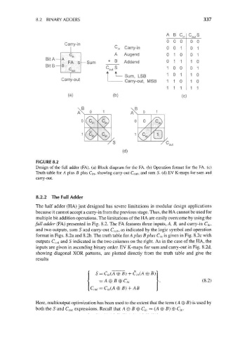
8.2 BINARY ADDERS                                                    337


                                                                       A B C, C_,,S
                                                                                 'out
                                                                       00 0      0 0
                              Carry-in            . ^ in Carry-in      0 0 1     Q 1
                                                       ~ .
                                                                        . . .
                             A FA s sum
                                                                        1 1
                      B!!B- i~                 + B Addend             ° 0 1 0    0 1
                                                  A
                                                      Augend
                                                                                 1 0
                                                                       1 0 0     0 1
                                                      Sum, LSB         1 0 1     1 0
                             Carry-out         I      Carry-out, MSB   1 1 0     1 0
                                                                       1 1 1     1 1
                               (a)                (b)                        (c)


                                                     (d)
                  FIGURE 8.2
                  Design of the full adder (FA), (a) Block diagram for the FA. (b) Operation format for the FA. (c)
                  Truth table for A plus B plus C\ n, showing carry-out C out, and sum S. (d) EV K-maps for sum and
                  carry-out.


                  8.2.2 The Full Adder
                  The half adder (HA) just designed has severe limitations in modular design applications
                  because it cannot accept a carry-in from the previous stage. Thus, the HA cannot be used for
                  multiple bit addition operations. The limitations of the HA are easily overcome by using the
                  full adder (FA) presented in Fig. 8.2. The FA features three inputs, A, B, and carry-in C in,
                  and two outputs, sum S and carry-out C our, as indicated by the logic symbol and operation
                  format in Figs. 8.2a and 8.2b. The truth table for A plus B plus C in is given in Fig. 8.2c with
                  outputs C out and S indicated in the two columns on the right. As in the case of the HA, the
                  inputs are given in ascending binary order. EV K-maps for sum and carry-out in Fig. 8.2d,
                  showing diagonal XOR patterns, are plotted directly from the truth table and give the
                  results


                                          S = C in(A ®B) + C in(A 0 B)
                                            = A 0 B 0 c in                            (8.2)


                  Here, multioutput optimization has been used to the extent that the term (A © B) is used by
                  both the S and C mi, expressions. Recall that A 0 B © C in = (A 0 B) 0 C in.