
Page 376 - Engineering Digital Design
P. 376
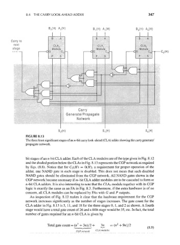
8.4 THE CARRY LOOK-AHEAD ADDER                                       347


                                                        Bl (H) A,(H)           B 0(H) A 0(H)


                                                                                             C 0(H)


                                               Carry
                                        Generate/Propagate
                                              Network


                                    S 2 (H)                  S,(H)                  S 0(H)
                  FIGURE 8.13
                  The three least significant stages of an n-bit carry look-ahead (CLA) adder showing the carry generate/
                  propagate network.


                  bit stages of an n-bit CLA adder. Each of the CLA modules are of the type given in Fig. 8.12
                  and the shaded portion below the CLAs in Fig. 8.13 represents the CGP network as required
                  by Eqs. (8.8). Notice that for Co(H) = 0(//), a requirement for proper operation of the
                  adder, one NAND gate in each stage is disabled. This does not mean that such disabled
                  NAND gates should be eliminated from the CGP network. All NAND gates shown in the
                  CGP network become necessary if m-bit CLA adder modules are to be cascaded to form m
                  n-bit CLA adders. It is also interesting to note that the CLA Q module together with its CGP
                  logic is exactly the same as an FA in Fig. 8.3. Furthermore, if the extra hardware is of no
                  concern, all CLA modules can be replaced by FAs with G and P outputs.
                    An inspection of Fig. 8.13 makes it clear that the hardware requirement for the CGP
                  network increases significantly as the number of stages increases. The gate count for the
                 CLA adder in Fig. 8.13 is 5, 11, and 18 for the three stages 0, 1, and 2 as shown. A fourth
                  stage would have a total gate count of 26 and a fifth stage would be 35, etc. In fact, the total
                 number of gates required for an n-bit CLA is given by

                                                                     2
                                              2
                              Total gate count = (n  + 3n)/2 +  3n^  = (n  + 9»)/2
                                              CGP network  CLA modules