
Page 377 - Engineering Digital Design
P. 377
348 CHAPTER 8 / ARITHMETIC DEVICES AND ARITHMETIC LOGIC UNITS (ALUs)
B 7. 4(H) A 7. 4(H) B 3. 0(H) A 3. 0(H)
\l 4\, 4l 4J, 4J, 4l
1 1 1 1 1 f
Carry to
n-1
stage
S,,.«(H) S 7. 4(H)
C 2 G, P,
G 2 P 2 C t G 0 P 0 C 0
CGP Network of Figure 8.13
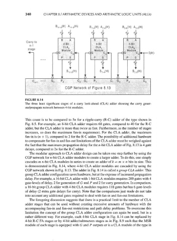
FIGURE 8.14
The three least significant stages of a carry look-ahead (CLA) adder showing the carry gener-
ate/propagate network between 4-bit modules.
This count is to be compared to 5n for a ripple-carry (R-C) adder of the type shown in
Fig. 8.5. For example, an 8-bit CLA adder requires 68 gates, compared to 40 for the R-C
adder, but the CLA adder is more than twice as fast. Furthermore, as the number of stages
increases, so does the maximum fan-in requirement. For the CLA adder, the maximum
fan-in is (n + 1), compared to 2 for the R-C adder. The possibility of additional hardware
to compensate for fan-in and fan-out limitations of the CLA adder must be weighed against
the fact that the maximum propagation delay for the n-bit CLA adder of Fig. 8.13 is 4 gate
delays, compared to 2n for the R-C adder.
The modular approach to CLA adder design can be taken one step further by using the
CGP network for n-bit CLA adder modules to create a larger adder. To do this, one simply
cascades m n-bit CLA modules in series to create an adder of k = m x n bits in size. This
is demonstrated in Fig. 8.14, where 4-bit CLA adder modules are cascaded by using the
CGP network shown in Fig. 8.13. The adder in Fig. 8.14 is called a group CLA adder. This
group CLA adder configuration saves hardware, but at the expense of increased propagation
delay. For example, a 16-bit CLA adder with 1-bit CLA modules requires 200 gates with 4
gate-levels of delay, 2 for generation of G and P and 2 for carry generation. In comparison,
a 16-bit group CLA adder with 4-bit CLA modules requires 118 gates but has 6 gate-levels
of delay (2 extra gate delays for carry). Note that the comparisons just made do not take
into account any additional gates required to deal with fan-in and fan-out limitations.
The foregoing discussion suggests that there is a practical limit to the number of CLA
adder stages that can be used without creating excessive amounts of hardware with the
accompanying fan-in and fan-out restrictions and path delay problems. To overcome this
limitation the concept of the group CLA adder configuration can again be used, but in a
rather different way. For example, each 4-bit CLA stage in Fig. 8.14 can be replaced by
4-bit R-C FA stages or by 4-bit adder/subtractors stages as in Fig. 8.9 such that the MSB
module of each stage is equipped with G and P outputs or is a CLA module of the type in