
Page 514 - Engineering Digital Design
P. 514
484 CHAPTER 10 / INTRODUCTION TO SYNCHRONOUS STATE MACHINE DESIGN
S H
( ) o-
Q(L) -
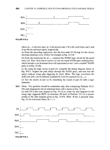
FIGUREP10.2
where Q t+\ is the next state, Q t is the present state, CKis the clock input, and S and
R are the set and reset inputs, respectively.
(a) From the preceding expression, plot the first-order EV K-map for this device
showing minimum cover. Follow the example in Fig. 10.1 Ib.
(b) From the expression for Q t+\, construct the NAND logic circuit for the gated
basic cell. Thus, show that it consists of four two-input NAND gates (nothing else),
which includes a set-dominant basic cell represented as two "cross-coupled" NAND
gates as in Fig. 10.18a.
(c) By using the logic circuit in part (b), complete the timing diagram shown in
Fig. P10.3. Neglect the path delays through the NAND gates, and note that the
arrows indicate rising edge triggering by clock. [Hint: The logic waveforms for
<2(H) and Q(L) can be deduced qualitatively from the equation for Q t+l.]
(d) Test the results of part (c) by simulating the circuit of part (b) with a logic
simulator.
10.4 (Note: This problem should be undertaken only after completing Problem 10.3.)
The state diagram for the set-dominant basic cell is shown in Fig. 10.12a.
(a) Add CK to this state diagram in Fig. 10.12a to create the state diagram for the
rising edge triggered (RET) set-dominant SR latch of Problem 10.3 in a manner
similar to the state diagram given in Fig. 10.47b. (Hint: If this is properly done,
Fig. 10.12a will result when CK = 1.)
Q(H)
Q(L) _
FIGURE P10.3