
Page 515 - Engineering Digital Design
P. 515
PROBLEMS 485
(b) Redesign the gated basic cell of Problem 10.3 by using the set-dominant basic
cell as the memory. To do this, follow the examples in Figs. 10.24, 10.25, and 10.47
by plotting EV K-maps for Set and Reset. Thus, it is necessary to combine the
information in the state diagram of part (a) with the excitation table in Fig. 10.15c
via the mapping algorithm given in Section 10.6.
(c) Construct the NAND/INV logic circuit from the results of part (a). In what way
does it differ from that constructed in part (b) of Problem 10.3? What can be said
about the S, R = 1,1 condition relative to these two designs? (Hint: Only one
inverter is used.)
(d) Read this circuit and write a single expression similar to that given in Problem
10.3. Then construct a first-order EV K-map from this result. Compare the K-map
with that in part (a) of Problem 10.3. Are these two K-maps the same? Explain your
answer.
(e) Complete the timing diagram in Fig. P10.3 for this design. What do you conclude
relative to the S, R = 1,1 condition?
(f) Test the results of part (d) by simulating the circuit of part (b) with a logic
simulator.
10.5 (a) By using Eq. (10.5), implement the set-dominant basic cell by using one 2-to-l
MUX and one AND gate (nothing else). [Hint: Plot Eq. (10.5) in a first-order K-map
of axis 5", and remember that the S and R inputs are introduced active low into the
basic cell.]
(b) Construct the logic circuit for the design of part (a). To do this, construct the logic
circuit for the 2-to-l MUX and provide both active high and active low outputs as
in Fig. 6.4d. Qualitatively, discuss how the mixed-rail output response of this design
compares with that of Fig. 10.18a.
10.6 (a) Convert an RET D flip-flop to a set-dominated RET SR flip-flop. To do this, use
minimum external logic and assume that the S and R inputs arrive active high.
(b) Complete the timing diagram in Fig. PI0.3 by simulating this flip-flop. Is mixed-
rail output response preserved in this flip-flop? Explain your answer.
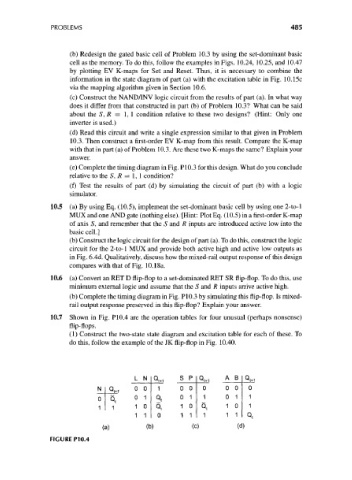
10.7 Shown in Fig. P10.4 are the operation tables for four unusual (perhaps nonsense)
flip-flops.
(1) Construct the two-state state diagram and excitation table for each of these. To
do this, follow the example of the JK flip-flop in Fig. 10.40.
L N S P Q A B
H1 0*1
0 0 0 0 0 0
Q*i ° °
0 1 0 1 1 0 1 1
Q t
1 1 0 1 0 Qt 1 0 1
1 1 1 1 1 1 1 Q»
(a) (b) (c) (d)
FIGURE P10.4