
Page 513 - Engineering Digital Design
P. 513
PROBLEMS 483
[6] H. Taub, Digital Circuits and Microprocessors. McGraw-Hill, New York, 1982.
[7] J. F. Wakerly, Digital Design Principles and Practices, 2nd ed. Prentice-Hall, Englewood Cliffs,
NJ, 1994.
[8] J. M. Yarbrough, Digital Logic Applications and Design. West Publishing Co., Minneapolis/St.
Paul, MN, 1997.
With the exception of texts by Katz and Taub, all of the previously cited references cover
adequately the subject of synchronous machine analysis. The texts by Fletcher, Shaw, and
Tinder in particular, present the subject in a fashion similar to that of the present text. Other
texts that can be recommended for further reading on this subject are those by Dietmeyer
and by Nelson et al., the former being more for the mathematically inclined.
[9] D. L. Dietmeyer, Logic Design of Digital Systems, 2nd ed. Allyn and Bacon, Inc., Boston, MA,
1978.
[10] V. P. Nelson, H. T. Nagle, B. D. Carroll, and J. D. Irwin, Digital Logic Circuit Analysis and
Design. Prentice Hall, Englewood Cliffs, NJ, 1995.
For detailed information on the subj ect of VHDL, the reader is referred to Further Reading
at the end of Chapter 6.
PROBLEMS
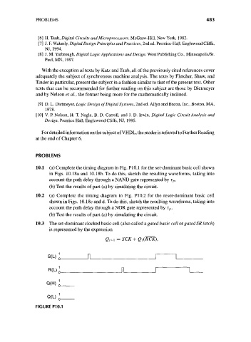
10.1 (a) Complete the timing diagram in Fig. P10.1 for the set-dominant basic cell shown
in Figs. 10.18a and 10.18b. To do this, sketch the resulting waveforms, taking into
account the path delay through a NAND gate represented by r p.
(b) Test the results of part (a) by simulating the circuit.
10.2 (a) Complete the timing diagram in Fig. P10.2 for the reset-dominant basic cell
shown in Figs. 10.18c and d. To do this, sketch the resulting waveforms, taking into
account the path delay through a NOR gate represented by T P.
(b) Test the results of part (a) by simulating the circuit.
10.3 The set-dominant clocked basic cell (also called a gated basic cell or gated SR latch)
is represented by the expression
=SCK+Q t(RCK),
FIGURE P10.1