
Page 516 - Engineering Digital Design
P. 516
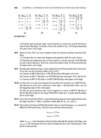
486     CHAPTER 10 / INTRODUCTION TO SYNCHRONOUS STATE MACHINE DESIGN


                            Q
                                             Q
                        QT» t*i  F G     Q t~* t+1  P K   Ql-» H1  S F     Q t^  Q t + 1  R M
                                                              Q
                         0-»0             0^ 0    1 0      0 -> 0  1 0      0^ 0   (J &
                         0-» 1            0-»1   ftfl      o-» 1  (S f)     0-M     1 1
                                                                  1^ 1j
                         1 -»0            1 -»0   1 ^      1 -»0            1 ->0   0 0
                                                                  11 0;
                         1 -»1            1 -»1   0 ^                       1 -> 1  (H
                                                           1 -»1
                              (a)              (b)              (c)              (d)
                     FIGURE P10.5


                          (2) Find the gate-minimum logic circuit required to convert any type D flip-flop to
                          each of these flip-flops. To do this, follow the model in Fig. 10.36 and assume that
                          all inputs arrive active high.

                     10.8  Shown in Fig. P10.5 are four excitation tables for unusual (perhaps nonsense) flip-
                          flops.
                          (1) Construct the two-state state diagram and operation table for each of these.
                          (2) Find the gate-minimum logic circuit required to convert any type of JK flip-flop
                          to each of these flip-flops. To do this, follow the model in Fig. 10.36 and assume that
                          all inputs arrive active high.
                     10.9  Find the gate-minimum logic circuit required for the following flip-flop conversions.
                          To do this, use the excitation tables in Fig. P10.5.
                          (a) Convert an MS D flip-flop to a MS FG flip-flop with inputs active low.
                          (b) Convert an RET T flip-flop to an FET PK flip-flop with inputs P(L) and K(H).
                          (c) Convert an RET D flip-flop to an RET RM flip-flop with inputs active high.
                     10.10 (a) Draw the two-state state diagram that describes the operation of an RET JK flip-
                          flop that has an active low synchronous clear input — one that takes effect only on
                          the triggering edge of the clock signal.
                          (b) Find the gate-minimum logic circuit required to convert an RET D flip-flop to
                          the JK flip-flop of part (a) by using NAND/INV logic only. Assume that the inputs
                          arrive active high.
                     10.11 Given the circuit in Fig. P10.6, complete the timing diagram to the right and determine
                          the logic function F. (Hint: Construct a truth table for Q\, Qi, and Z.)
                    10.12 The results of testing an FSM indicate that when its clock frequency fcK exceeds 25
                          MHz the FSM misses data. The tests also yield the following data:


                                                    tFF(ma\) = 15 HS
                                                     ^MS(max) = 13 IIS,

                          where T/7/r (max) is the maximum observed delay through the memory flip-flops, and
                          r/v5( max) is the maximum observed delay through the next-state-forming logic, both
                          given in nanoseconds.