
Page 585 - Engineering Digital Design
P. 585
PROBLEMS 555
Sanity
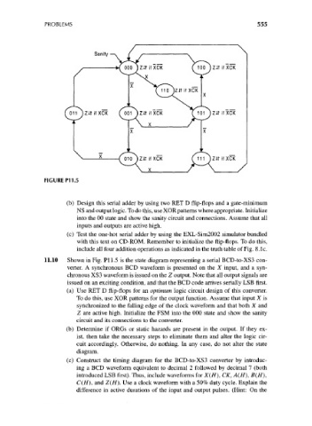
FIGURE P11.5
(b) Design this serial adder by using two RET D flip-flops and a gate-minimum
NS and output logic. To do this, use XOR patterns where appropriate. Initialize
into the 00 state and show the sanity circuit and connections. Assume that all
inputs and outputs are active high.
(c) Test the one-hot serial adder by using the EXL-Sim2002 simulator bundled
with this text on CD-ROM. Remember to initialize the flip-flops. To do this,
include all four addition operations as indicated in the truth table of Fig. 8. Ic.
11.10 Shown in Fig. PI 1.5 is the state diagram representing a serial BCD-to-XS3 con-
verter. A synchronous BCD waveform is presented on the X input, and a syn-
chronous XS3 waveform is issued on the Z output. Note that all output signals are
issued on an exciting condition, and that the BCD code arrives serially LSB first.
(a) Use RET D flip-flops for an optimum logic circuit design of this converter.
To do this, use XOR patterns for the output function. Assume that input X is
synchronized to the falling edge of the clock waveform and that both X and
Z are active high. Initialize the FSM into the 000 state and show the sanity
circuit and its connections to the converter.
(b) Determine if ORGs or static hazards are present in the output. If they ex-
ist, then take the necessary steps to eliminate them and alter the logic cir-
cuit accordingly. Otherwise, do nothing. In any case, do not alter the state
diagram.
(c) Construct the timing diagram for the BCD-to-XS3 converter by introduc-
ing a BCD waveform equivalent to decimal 2 followed by decimal 7 (both
introduced LSB first). Thus, include waveforms for X(H), CK, A(H), B(H\
C(H), and Z(H). Use a clock waveform with a 50% duty cycle. Explain the
difference in active durations of the input and output pulses. (Hint: On the