
Page 584 - Engineering Digital Design
P. 584
554 CHAPTER 11 / SYNCHRONOUS FSM DESIGN CONSIDERATIONS
D flip-flops to be used for the synchronizer. Consider that at 200 MHz, it is
necessary to use a synchronizing scheme of the type shown in Fig. 11.23a for
which a divide-by-4 counter is used in the diagram.
(a) Calculate the MTBF (in seconds, days and years) if r — 0.5 ns and T 0 =
6
1 x 10~ seconds. [Hint: Use Eq. (11.3) and take into account the cumulative
effects of both stages.]
(b) Repeat part (a) if a divide-by-two counter is used in the diagram. Calculate
the MTBF in seconds for comparison with the result in part a.
11.7 It is desired to find a safe operating clock frequency for a given FSM. The following
data is collected relative to the operation of the FSM:
Flip-flop parameters f pi h = 6 ns; f pM = 9 ns
Maximum delay through the NS logic T NS = 1 ns
Maximum flip-flop setup time t su = 3 ns
Calculate a safe operating clock frequency fcK based on a 15% safety factor.
11.8 Derive the expressions for Vx(t) in Eqs. (11.8) and (11.9) relative to Fig. 11.31c.
Assume that R\ ^> R2 and that the switch is opened (or closed) at time t = 0 only
after steady-state conditions are reached. State any simplifying assumptions that
are made relative to the Schmitt trigger and inverter. (Note: This exercise involves
solving a first-order RC circuit.)
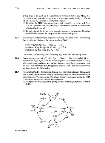
11.9 Presented in Fig. PI 1.4 is the state diagram for a one-bit serial adder. The operand
bits, a and b, are introduced serially and are synchronized antiphase to the clock
triggering edge. The outputs are S (sum) and C 0 (carry-out). Assume that the FSM
is initialized (reset) after each addition operation.
(a) Complete the state diagram by giving it a state code assignment that is free of
ORGs.
C IT
FIGURE P11.4