
Page 583 - Engineering Digital Design
P. 583
PROBLEMS 553
S+T
ST
S©T
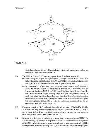
FIGURE P11.3
static hazard cover (if any). Do not alter the state code assignment and do not
construct a logic circuit for the FSM.
11.4 The FSM in Figure PI 1.3 has two inputs, S and T and one output, P.
(a) Run a complete output race glitch (ORG) analysis on this FSM. To do this,
follow the examples in Section 11.2. Thus, if ORGs exist, indicate their origin
and type (4- or —). Do not alter the state diagram in any way.
(b) In consideration of part (a), run a complete static hazard analysis on this
FSM. To do this, follow the examples in Section 11.3. However, it is not
known whether to use NAND- or NOR-based flip-flops for its design. Consider
both SOP and POS output-forming logic and give the gate/input tally for
each (including any static hazard cover). Based on this information, make a
selection as to the type of flip-flop (NAND- or NOR-based) that will yield
the most optimum design. Do not alter the state code assignment and do not
construct a logic circuit for the FSM.
11.5 Carry out complete ORG and static hazard analyses on the FSM in Fig. 11.43b.
To do this, use may be made of the NS and output expressions in Eqs. (11.11). If
any of these timing defects exist in the output signals, indicate the best means of
eliminating them. (Hint: See Subsection 11.2.2.)
11.6 Suppose it is desirable to estimate the mean time between failures (MTBF) for
a synchronizing system that is required to protect a hypothetical FSM operated
at 200 MHz when the asynchronous data change at an average rate of 10 kHz.
By experiment, the average setup time t su is 1 nanosecond (ns) for the high-speed