
Page 645 - Engineering Digital Design
P. 645
13.2 ARCHITECTURES CENTERED AROUND NONREGISTERED PLDs 615
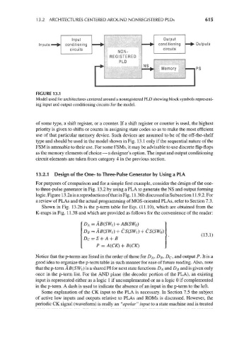
Inputs' Outputs
NON-
REGISTERED
r
PLD
FIGURE 13.1
Model used for architectures centered around a nonregistered PLD showing block symbols represent-
ing input and output conditioning circuits for the model.
of some type, a shift register, or a counter. If a shift register or counter is used, the highest
priority is given to shifts or counts in assigning state codes so as to make the most efficient
use of that particular memory device. Such devices are assumed to be of the off-the-shelf
type and should be used in the model shown in Fig. 13.1 only if the sequential nature of the
FSM is amenable to their use. For some FSMs, it may be advisable to use discrete flip-flops
as the memory elements of choice — a designer's option. The input and output conditioning
circuit elements are taken from category 4 in the previous section.
13.2.1 Design of the One- to Three-Pulse Generator by Using a PLA
For purposes of comparison and for a simple first example, consider the design of the one-
to three-pulse generator in Fig. 13.2 by using a PLA to generate the NS and output forming
logic. Figure 13.2a is a reproduction of that in Fig. 11.36b discussed in Subsection 11.9.2. For
a review of PLAs and the actual programming of MOS-oriented PLAs, refer to Section 7.3.
Shown in Fig. 13.2b is the p-term table for Eqs. (11.10), which are obtained from the
K-maps in Fig. 11.38 and which are provided as follows for the convenience of the reader:
D A=AB(SW l)+AB(SW 0)
D B = AB(SWi) + CS(SWi)
(13.1)
DC = S + A + B
P = A(CK) + B(CK)
Notice that the p-terms are listed in the order of those for D^, DB, DC, and output P. It is a
good idea to organize the p-term table in such manner for ease of future reading. Also, note
that the p-term AB(S W\) is a shared PI for next state functions DA and D B and is given only
once in the p-term list. For the AND plane (the decoder portion of the PLA), an existing
input is represented either as a logic 1 if uncomplemented or as a logic 0 if complemented
in the p-term. A dash is used to indicate the absence of an input in the p-term to the left.
Some explanation of the CK input to the PLA is necessary. In Section 7.5 the subject
of active low inputs and outputs relative to PLAs and ROMs is discussed. However, the
periodic CK signal (waveform) is really an "apolar" input to a state machine and is treated