
Page 646 - Engineering Digital Design
P. 646
616 CHAPTER 13 /ALTERNATIVE SYNCHRONOUS FSM ARCHITECTURES
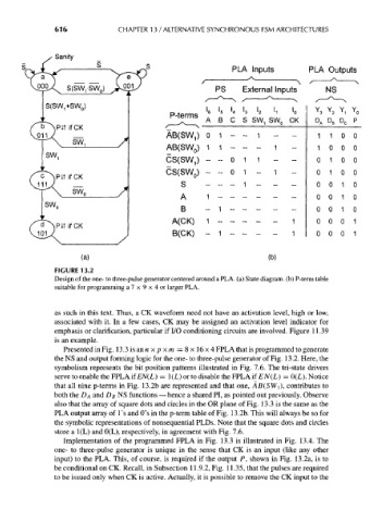
Sanity
PLA Inputs
/ \
S(SW 1-SW 0) PS External Inputs
S(SW 1+SW 0)
P-terms D'
A B C S SW 1 SW 0 CK p
D B D c
Pit ifCK
AB(SW.,) 0 1 - -- 1 1 1 0 0
AB(SW 0) 1 1 _____ _ i 1 0 0 0
CSCSW,) - - 0 1 1 0 1 0 0
CS(SW 0) - -01- 1 0 1 0 0
s 1 - 0 0 1 0
A 1 0 0 1 0
B - 1 0 0 1 0
A(CK) "I __ __ __ __ __ "I 0 0 0 1
B(CK) 1 1 1 1 0 0 0 1
(a) (b)
FIGURE 13.2
Design of the one- to three-pulse generator centered around a PLA. (a) State diagram, (b) P-term table
suitable for programming a 7 x 9 x 4 or larger PLA.
as such in this text. Thus, a CK waveform need not have an activation level, high or low,
associated with it. In a few cases, CK may be assigned an activation level indicator for
emphasis or clarification, particular if I/O conditioning circuits are involved. Figure 11.39
is an example.
Presented in Fig. 13.3 is an n x /> x m = 8x16x4 FPLA that is programmed to generate
the NS and output forming logic for the one- to three-pulse generator of Fig. 13.2. Here, the
symbolism represents the bit position patterns illustrated in Fig. 7.6. The tri-state drivers
serve to enable the FPLA ifEN(L) = 1 (L) or to disable the FPLA if EN(L) = 0(L). Notice
that all nine p-terms in Fig. 13.2b are represented and that one, AB(SWi), contributes to
both the DA and DB NS functions — hence a shared PI, as pointed out previously. Observe
also that the array of square dots and circles in the OR plane of Fig. 13.3 is the same as the
PLA output array of 1's and O's in the p-term table of Fig. 13.2b. This will always be so for
the symbolic representations of nonsequential PLDs. Note that the square dots and circles
store a 1(L) and 0(L), respectively, in agreement with Fig. 7.6.
Implementation of the programmed FPLA in Fig. 13.3 is illustrated in Fig. 13.4. The
one- to three-pulse generator is unique in the sense that CK is an input (like any other
input) to the PLA. This, of course, is required if the output P, shown in Fig. 13.2a, is to
be conditional on CK. Recall, in Subsection 11.9.2, Fig. 11.35, that the pulses are required
to be issued only when CK is active. Actually, it is possible to remove the CK input to the