
Page 650 - Engineering Digital Design
P. 650
620 CHAPTER 13 / ALTERNATIVE SYNCHRONOUS FSM ARCHITECTURES
ROM Inputs ROM Outputs
/ / '^ — \
External
PS Inputs
s~ _/\_ ~N ^-^-N
'5 u >3 '1 Y 1 Y 0
I 0
' 2
A B c s sw, sw- D. D» n r P
0 0 0 0 X X 0 0 0 0
0 0 0 1 0 0 0 0 1 0
\ S SW SW 0
p 1 1 0 1 1
ABC\ 000 001 011 010 110 111 101 100 0 0 0 X 0
000 000 000 000 000 011 011 011 001 0 0 0 0 1 0 1 0 1 1 0
011 001 001 111 111 111 111 001 001 1 0 1 1 X 0 X 0 0 1 1
111 001 101 101 001 001 101 101 001 1 0 1 1 X 1 X 1 1 1 1
101 001 001 001 001 001 001 001 001 1 1 1 1 X X 0 0 0 1 1
001 000 000 000 000 001 001 001 001 0 1 1 1 X X 1 1 0 1 1
1 0 1 X X X 0 0 1 1
SW 0 SW 0 0 1 1 0 1
0 X X 0 0
(a) 0 0 1 0 X X 0 0 0 0
X's • X's p* \ < J's
x = Irrelevant input ^ = Don't care
(b)
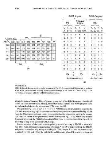
FIGURE 13.6
ROM design of the one- to three-pulse generator in Fig. 13.2, except with CK removed as an input
to the ROM. (a) State table showing an unconditional output P for states b, c, and d in Fig. 13.2a.
(b) Collapsed program table for a PROM implementation.
a logic 0; it doesn't matter. This, of course, is true only if the FSM is properly initialized,
in this case into the 000 state. Finally, remember that all outputs in a ROM program table
are indicated relative to the present state (PS), never the NS.
6
Presented in Fig. 13.7 is a 2" x m = 2 x 4 PROM that is programmed to generate the
NS- and output-forming logic for the one- to three-pulse generator represented in Fig. 13.6b.
Here, the filled square dots and circles represent the fusible bit position patterns for storage
of 1's and O's shown in the generalized PROM structure of Fig. 7.2. As before, the tri-state
driver outputs permit the PROM to be enabled if EN(L) = 1(L) or disabled if EN(L) = 0(L),
according to Fig. 3.8d, assuming CMOS logic.
Implementation of the one- to three-pulse generator by using a PROM is shown in
Fig. 13.8. Here, the required dependence of output P on CK is removed from the PROM
and placed external to it by using an AND gate. Thus, output P' cannot be issued except
in states Oil, 111, and 101 of the state table, and then only when CK is active, as required