
Page 654 - Engineering Digital Design
P. 654
624 CHAPTER 13 / ALTERNATIVE SYNCHRONOUS FSM ARCHITECTURES
reader can verify this by comparing the ROM program tables in Figs. 13.6b and IS.lOb
with their respective state table and state diagram in Figs. 13.6a and 13.10a.
The ROM program table in Fig. 13.1 Ob could have been constructed from a state table.
However, this approach would have been more difficult, or at least more tedious, mainly
because of the size of the state table needed. Nevertheless, a state table can be constructed
by using state identifiers, thereby permitting the construction of the ROM program table to
proceed with little effort. Use of a state table for this purpose is the method of choice if a
CAD approach is used.
8
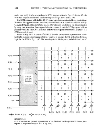
Shown in Fig. 13.11 is an 8-to-2 EPROM decoder and symbolic representation of the
fusible bit position patterns in the OR plane required to generate the NS- and output-forming
logic for the FSM in Fig. 13.10. The meaning of the filled squares and circles and use of
EN(L).
D A(H) D B(H) D C{H) M(H) N(H) P(H) Q(H)
Stores a 1(L) —O— Stores a 0(L)
FIGURE 13.11
EPROM decoder and symbolic representation of the fusible bit position patterns in the OR plane
required to program the fictitious FSM in Fig. 13.10.