
Page 658 - Engineering Digital Design
P. 658
628 CHAPTER 13 / ALTERNATIVE SYNCHRONOUS FSM ARCHITECTURES
indicated by shaded loops, yields the expressions:
S] = X + C + D
(13.2)
L = D
where R = 0 or 1 and PA = PB = PC = PD = 0 by inspection of the state diagram in
Fig. 13.13a. The logic for L can also be deduced from an inspection of the state diagram
since state variable D toggles in complementary fashion with respect to the left shifting
of 1's and O's. Observe that state pairs, 0101 and 1010, are the only two four-bit patterns
that can be cycled exclusively with either a left shift or a right shift. Knowledge of this
fact can be useful in state machine designs centered around a shift register, as in this case.
Implementation of Eqs. (13.2) is shown in Fig. 13.14b, where the Moore output is simply
Z(//) = A(H), as deduced from the state diagram in Figure 13.13a.
S
Sanity
Synchronous Inputs
S(H),T(H),U(L),V(H)
V(SRO)
Outputs
MIT if V M(H), N(L), P(H), Q(H)
0 0 (H)-Hold
0 1 (SR)-Shift Right
1 0 (SL)--Shift Left
1 1 (PL)-Parallel load
NIT if V
(a) (b)
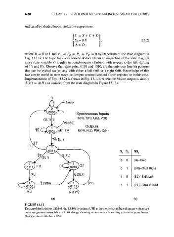
FIGURE 13.15
Design of the fictitious FSM of Fig. 13. lOa by using a USR as the memory, (a) State diagram with a state
code assignment amenable to a USR design showing state-to-state branching actions in parentheses,
(b) Operation table for a USR.