Page 657 - Engineering Digital Design
P. 657

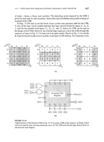
13.3  STATE MACHINE DESIGNS CENTERED AROUND A SHIFT REGISTER        627


                  of states — hence, a linear state machine. The branching action required by the USR is
                  given for each state-to-state transition. Notice that only left shifting and parallel loading are
                  required of the USR.
                    In Figs. 13.13b and (c) are the block circuit symbol and operation table for the USR.
                  A view of the logic circuit symbol indicates that logic must be found for inputs S\, SQ, R,
                  L, and the four parallel load inputs P A, P B, P c, and P D before the USR can be used in
                  the design of this FSM. However, the external logic required to drive the USR through the
                  sequence of states in Fig. 13.13a turns out to be quite simple. Shown in Fig. 13.14a are the
                  K-maps for the two mode controls and the serial input for left shifting. The minimum cover,


          \CD                          VCD                                 \CD
        ABX 00     01   11   10      AB \ 00     01  11   10             AB\ 00     01   11   10
                                                      ^
           00                           00  0    0         0                00
           01                           01       X    (f)                   01
                                            *              ^l
           11                           11  <!> * $        ^J               11
                                            </> ^ *
           10                           10                 0                10
                                                            rs (


                                                         (a)


                                                                      U(H)
                                 X(H)              P *  r P B  r P  r F > D
                                                   r
                                      ±T^V-
                                                             C
                                                 1
                                 D(HH / "
                            B(H) ^         A_
                                                 0
                                                      Universal Shift
                                                        Register     CL D — Sar
                                         CK— C  >
                                                                        •**<y
                                        0(H)    R                     L       -D(H)
                                                             QC   C
                                                   QI M  Q 8 D  W
                                                                  r —
                                                                               Z(H)
                                                  A(H) B(H) C(H) D(H)

                                                        (b)
                  FIGURE 13.14
                  Implementation of the fictitious FSM in Fig. 13.13 by using a USR as the memory, (a) Mode control
                  and serial input K-maps showing minimum cover, (b) The USR and external logic derived from (a)
                  and from the state diagram.
   652   653   654   655   656   657   658   659   660   661   662