
Page 653 - Engineering Digital Design
P. 653
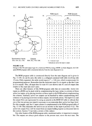
13.2 ARCHITECTURES CENTERED AROUND NONREGISTERED PLDs                623


                                                          ROM Inputs          ROM Outputs
                                                                          /               \
                                    Sanity
                                                         PS                 NS
                                                                          / —-*  ^
                                                       IB  's  '4  '3  '2  '1  >o  Y 6  Y T  3  Y T  2  T Y 1
                                                       A  B c s  T u* V   DA  D B DC  M N* p  Q
                                                       0  0  0  0  X  X  X  0  0  0  0  0  0  0
                                                       0  0  0  1  X  X  X  0  0  1  0  0  0  0
                                                       0  0  1  X  0  X  0  0  0  1  0  0  0  0
                                                       0  0  1  X  X  X  1  0  0  0  1  0  0  0
                                                       0  0  1  X  1  X  0  1  0  1  0  0  0  0
                                                       1  0  1  0  0  X  X  0  0  0  0  0  0  0
                                                       1  0  1  0  1  X  X  1  1  1  0  0  0  0
                                                       1  0  1 1  X  X  X  1  1  0  0  0  0  0
                                                       1  1  0  X  X  1  X  1  1  0  0  0  0 1
                                                       1  1  0  X  X  0  X  1  0  0  0  0  0  1
                                                       1  1  1  X  X  X  X  0  1  0  0  0  1  0
                                                       0  1  0  X  0  X  X  1 1  0  1  0  0  0
                                                       0  1  0  X  1  X  X  0  1  0  1  0  0  0
                    MiT
                                                       1  0  0  X  X  X  0  1  0  1  0 1  0  0
                                                       1  0  0  X  X  X  1  1  0  1  0  0  0  0
                Synchronous Inputs   Outputs
                 S(H), T(H), U(L), V(H)  M(H), N(L), P(H), Q(H)  X = Irrelevant input
                                                        * Indicates an active low input or output
                  FIGURE 13.10
                  Design of the NS and output logic for a fictitious FSM by using a ROM. (a) State diagram, (b) Coll-
                  apsed ROM program table constructed directly from the state diagram in (a).


                    The ROM program table is constructed directly from the state diagram and is given in
                  Fig. 13.10b. As can be seen, this table is a collapsed canonical truth table involving only
                                                          7
                  15 rows. Fully expanded, this table would require 2  = 128 rows, which is unnecessary for
                  programming purposes. Remember that the irrelevant input X is to inputs as the don't care
                  0 is to outputs. Thus, all input data for state 011 (not shown) take X's and all output data
                  relative to this state take don't cares.
                    There are other features of this ROM program table that are noteworthy. Active low
                  inputs to a ROM can be dealt with by complementing the logic values in columns of those
                  active low inputs, or by placing inverters on these inputs to the ROM and not complementing
                  the columns. Similarly, active low outputs can be handled by either complementing their
                  columns or by placing an inverter on these outputs, but not both actions. The input U(L) and
                  the output N(L) are represented by using an asterisk in the ROM I/O table to indicate that
                  one of the two actions just stated is necessary to accommodate their active low logic level.
                  For this example, only the U input column is complemented in the ROM program table of
                  Fig. 13.10b. This eliminates the need to use an inverter on the input to produce U(L). The
                  active low output N(L) will be issued from an output holding register as discussed later in
                  this section. Section 7.5 provides a review of this subject.
                    One other feature of the ROM program table, mentioned earlier, is important to remem-
                  ber: The outputs are always given relative to the present state, never the next state. The