
Page 649 - Engineering Digital Design
P. 649
13.2 ARCHITECTURES CENTERED AROUND NONREGISTERED PLDs 619
A(H) B(H) C(H) S(H) SW^H) SW 0(H) CK
I 7(H) I 6(H) I 5(H) I 4(H) I 3(H) I 2(H) I^H) I 0(H)
Non-programmable OR
Plane
XV
AB(SW 1)-
AB(SW 0)-
ABfSW,)-
CS(SW 0)-
S-
A-
B-
A(CK)-
B(CK)-
EN(L)
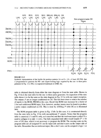
FIGURE 13.5
Symbolic representation of the fusible bit position patterns for an 8 x 16 x 4 basic I/O PAL that
is programmed to generate the NS- and output-forming logic required by the one- to three-pulse
generator in Fig. 13.2. PAL is a registered trademark of AMD, Inc.
table is obtained directly from either the state diagram or from the state table. Shown in
Fig. 13.6a is the state table for the one- to three-pulse generator. An inspection of the state
table shows it to be the same as the state diagram in Fig. 13.2a with one major exception.
The outputs P are no longer conditional on CK. This has been done to reduce the number
of inputs to the ROM, PROM in this case. Recall that ROM size increases by a factor of
2 for each additional ROM input. Now, however, another means must be found to produce
a pulse output conditional on CK. This is done by ANDing P with CK as is illustrated
later.
The ROM program table is given in Fig. 13.6b. In this case, it is constructed directly
from the state table in Fig. 13.6a with unconditional P outputs. Notice that the program
table is canonical (1's and O's only, as it must be) and that the irrelevant input symbol X is
6
used to collapse it to only 11 rows. The fully expanded truth table would require 2 = 64
rows of I/O data, which is not necessary to program the ROM. The missing states in the
program table are all assigned X's on the input side and don't-cares on the output side of
the table. Remember that an irrelevant input, like a don't care, can be assigned a logic 1 or