
Page 647 - Engineering Digital Design
P. 647
13.2 ARCHITECTURES CENTERED AROUND NONREGISTERED PLDs 617
or ^ $ or Input to p-term
r
A(H) B(H) C(H) S(H) SW^H) SW 0(H) CK —J—Stores a 1 (L)
I 7(H) I 6(H) I 5(H) I 4(H) I 3(H) I 2(H) I^H) I 0(H)
Stores a 0(L)
AB(SW 1)-
AB(SW 0)-
CS(SW 0)-
s-
A-
B-
A(CK)-
B(CK)-
EN(L) -
D A(H) D B(H) D C(H) P(H)
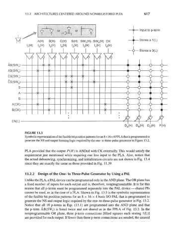
FIGURE 13.3
Symbolic representation of the fusible bit position patterns for an 8 x 1 6 x 4 FPL A that is programmed to
generate the NS and output forming logic required by the one- to three-pulse generator in Figure 13.2.
PLA provided that the output P(H} is ANDed with CK externally. This would satisfy the
requirement just mentioned while requiring one less input to the PLA. Also, notice that
the actual debouncing, synchronizing, and initialization circuits are not shown in Fig. 13.4
since they are exactly the same as those provided in Fig. 1 1.39.
1 3.2.2 Design of the One- to Three-Pulse Generator by Using a PAL
Unlike the PLA, a PAL device can be programmed only in the AND plane. The OR plane has
a fixed number of inputs for each output and is, therefore, nonprogrammable. It is for this
reason that all p-terms must be programmed separately into the PAL device — shared Pis
cannot be used, as in the case of a PLA. Shown in Fig. 13.5 is the symbolic representation
of the fusible bit position patterns for an 8 x 16 x 4 basic I/O PAL that is programmed to
generate the NS and output logic required by the one- to three-pulse generator in Fig. 13.2.
Notice that all 10 p-terms in Eqs. (13.1) are programmed into the AND plane and that
the p-term AB(SW\) is listed twice and not shared as in the FPLA of Fig. 13.3. In the
nonprogrammable OR plane, three p-term connections [filled squares each storing 1(L)]
are provided for each output. If fewer than three p-term connections are needed, the unused