
Page 648 - Engineering Digital Design
P. 648
618 CHAPTER 13 / ALTERNATIVE SYNCHRONOUS FSM ARCHITECTURES
CK
SW 0(H)
SW/H)
7
V ; r
S(H) — Debouncing and
synchronizing circuits
EN(L) Sanity(L)
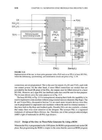
FIGURE 13.4
Implementation of the one- to three-pulse generator with a PLD such as an FPLA or basic I/O PAL,
where the debouncing, synchronizing, and initialization circuits are given in Fig. 11.39.
connections are not programmed. This is the case for outputs DA(H) and P(H), each with
one unused p-term. On the other hand, if more ORed connections are needed than are
provided by the fixed OR plane of the PAL, the outputs must be ORed external to a basic
I/O PAL. However, an L-type PAL has feedback paths that could be used for that purpose.
The tri-state drivers serve the same purpose as in Fig. 13.3.
The basic I/O PAL in Fig. 13.5 is nonregistered, meaning that it lacks the capability to be
used to implement a state machine without using external memory elements (flip-flops). The
R- and V-type PALs, discussed in Section 7.4, are much more versatile devices since they
can be programmed to implement state machines without the need for external memory —
they have built-in flip-flops and feedback paths. Erasable PALs are also available, a feature
that makes them even more attractive to the designer. The acronym PAL is a registered
trademark of Advanced Micro Devices, Inc. Therefore, use of this acronym acknowledges
AMD's right of trademark for all PAL-type devices.
13.2.3 Design of the One- to Three-Pulse Generator by Using a ROM
Whereas the PAL is programmed in the AND plane, the ROM is programmed only in the OR
plane. But programming the ROM is simpler in the sense that the canonical ROM program