
Page 651 - Engineering Digital Design
P. 651
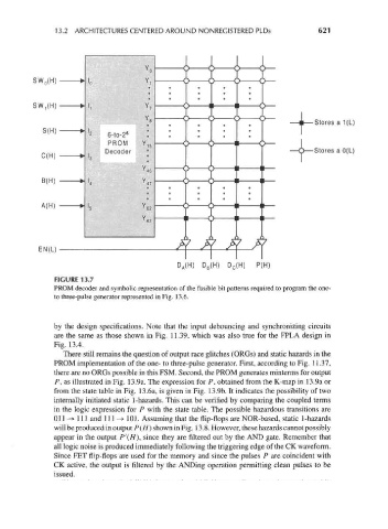
13.2 ARCHITECTURES CENTERED AROUND NONREGISTERED PLDs                621


              EN(L)

                                                 D A (H) D B(H) D C (H)  P(H)
                  FIGURE 13.7
                 PROM decoder and symbolic representation of the fusible bit patterns required to program the one-
                 to three-pulse generator represented in Fig. 13.6.


                 by the design specifications. Note that the input debouncing and synchronizing circuits
                  are the same as those shown in Fig. 11.39, which was also true for the FPLA design in
                 Fig. 13.4.
                    There still remains the question of output race glitches (ORGs) and static hazards in the
                 PROM implementation of the one- to three-pulse generator. First, according to Fig. 11.37,
                 there are no ORGs possible in this FSM. Second, the PROM generates minterms for output
                  P, as illustrated in Fig. 13.9a. The expression for P, obtained from the K-map in 13.9a or
                 from the state table in Fig. 13.6a, is given in Fig. 13.9b. It indicates the possibility of two
                 internally initiated static 1-hazards. This can be verified by comparing the coupled terms
                 in the logic expression for P with the state table. The possible hazardous transitions are
                 Oil —> 111 and 111 -> 101. Assuming that the flip-flops are NOR-based, static 1-hazards
                 will be produced in output P(H) shown in Fig. 13.8. However, these hazards cannot possibly
                 appear in the output P'(H), since they are filtered out by the AND gate. Remember that
                 all logic noise is produced immediately following the triggering edge of the CK waveform.
                 Since FET flip-flops are used for the memory and since the pulses P are coincident with
                 CK active, the output is filtered by the ANDing operation permitting clean pulses to be
                 issued.