
Page 655 - Engineering Digital Design
P. 655
13.2 ARCHITECTURES CENTERED AROUND NONREGISTERED PLDs 625
0(H) 0(H) Sanity(L)
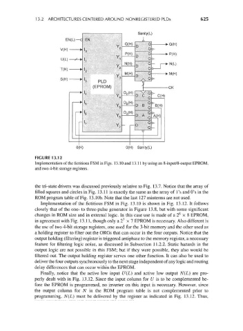
FIGURE 13.12
Implementation of the fictitious FSM in Figs. 13.10and 13.11 by using an 8-input/8-output EPROM,
and two 4-bit storage registers.
the tri-state drivers was discussed previously relative to Fig. 13.7. Notice that the array of
filled squares and circles in Fig. 13.11 is exactly the same as the array of 1's and O's in the
ROM program table of Fig. 13.1 Ob. Note that the last 127 minterms are not used.
Implementation of the fictitious FSM in Fig. 13.10 is shown in Fig. 13.12. It follows
closely that of the one- to three-pulse generator in Figure 13.8, but with some significant
8
changes in ROM size and in external logic. In this case use is made of a 2 x 8 EPROM,
7
in agreement with Fig. 13.11, though only a 2 x 7 EPROM is necessary. Also different is
the use of two 4-bit storage registers, one used for the 3-bit memory and the other used as
a holding register to filter out the ORGs that can occur in the four outputs. Notice that the
output holding (filtering) register is triggered antiphase to the memory register, a necessary
feature for filtering logic noise, as discussed in Subsection 11.2.2. Static hazards in the
output logic are not possible in this FSM; but if they were possible, they also would be
filtered out. The output holding register serves one other function. It can also be used to
deliver the four outputs synchronously to the next stage independent of any logic and routing
delay differences that can occur within the EPROM.
Finally, notice that the active low input U(L) and active low output N(L) are pro-
perly dealt with in Fig. 13.12. Since the input column for U is to be complemented be-
fore the EPROM is programmed, no inverter on this input is necessary. However, since
the output column for N in the ROM program table is not complemented prior to
programming, N(L) must be delivered by the register as indicated in Fig. 13.12. Thus,