
Page 663 - Engineering Digital Design
P. 663
632 CHAPTER 13 / ALTERNATIVE SYNCHRONOUS FSM ARCHITECTURES
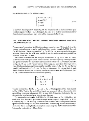
output-forming logic in Eqs. (13.4) becomes
M = BCDV+BD
N = BCDV
(13.5)
P=BC
Q = CD
as read from the composite K-map in Fig. 13.16c. This represents an increase of three gates
over that required by Eqs. (13.4). But again, the price to be paid for convenience and for
the reduction in external gate logic is the added state decoder hardware.
13.4 STATE MACHINE DESIGNS CENTERED AROUND A PARALLEL LOADABLE
UP/DOWN COUNTER
For purposes of comparison, it will be interesting to design the same FSMs as in Section 13.3
but now centered around a parallel loadable up/down counter instead of a USR. Shown in
Fig. 13.18a is the "linear state machine" of Fig. 13.13a, but now state coded in a count
sequence. Notice that the MSB state variable is inactive and that only one parallel load
transition exists, 0011 ->• 0000.
The counter to be used for this design is that featured in Fig. 12.23. This is a binary
up/down counter with synchronous parallel load and true hold capability. The logic symbol
and operation table for this counter are reproduced from Subsection 12.3.4 and are presented
in Figs. 13.18b and 13.18c for convenience of the reader. An inspection of the logic circuit
symbol indicates that external logic must be found for inputs S\, SQ, Up, Dn, and the four
parallel load inputs PA, PB, PC, and P D. But, as it turns out, this external logic is quite
simple. From the K-maps and minimum cover for the mode control and Up/Dn inputs given
in Fig. 13.19a, there results the external logic given by
S l=CDX
S 0 = X + B
(13.6)
Up = B
Dn = B
where it is understood that P A = PB = PC — PD = 0 by inspection of the state diagram
in Fig. 13.18a. That is, the parallel load inputs are necessarily all zero because the only
parallel load branching is from state 0011 to state 0000. Notice that the logic for Up and
Dn could also have been deduced from the state diagram.
The resulting logic circuit for the FSM in Fig. 13.18a is shown in Fig. 13.19b. Here, it is
easily seen from the state diagram that the single Moore output is simply Z(//) = B(H).
Comparing Fig. 13.19b with Fig. 13.14b indicates that both a USR and parallel loadable
up/down counter design of this linear state machine result in only minimal external logic.
Remember that to accomplish these designs it is necessary that the USR and counter have
both parallel load and true hold capability.