
Page 664 - Engineering Digital Design
P. 664
p p p p
~A r B ~C r D
S,
CL O-
4-Bit Parallel
S 0 0 0 Q, True hold
)> Loadable Up/Down
Binary Counter ,.„
nn
v x/ U P 0 1 Tj Up/down count
BO Dn
QA QB QC QO 1 X P, Parallel load
(b) (c)
(a)
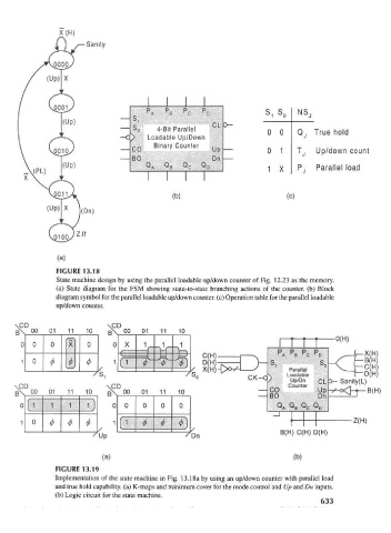
FIGURE 13.18
State machine design by using the parallel loadable up/down counter of Fig. 12.23 as the memory.
(a) State diagram for the FSM showing state-to-state branching actions of the counter, (b) Block
diagram symbol for the parallel loadable up/down counter, (c) Operation table for the parallel loadable
up/down counter.
CD
00 01
-0(H)
P
A PB PC PD
S 0
Parallel
Loadable D(H)
Up/Dn CL >- Sanity(L) v
r
/
_ _ Counter ,, '
CO Up B(H)
BO Dn
QA QB QC QD
-Z(H)
B(H)C(H)D(H)
(a) (b)
FIGURE 13.19
Implementation of the state machine in Fig. 13.18a by using an up/down counter with parallel load
and true hold capability, (a) K-maps and minimum cover for the mode control and Up and Dn inputs.
(b) Logic circuit for the state machine.
633