
Page 665 - Engineering Digital Design
P. 665
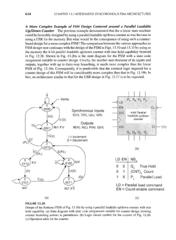
634              CHAPTER 1 3 / ALTERNATIVE SYNCHRONOUS FSM ARCHITECTURES


                    A More Complex Example of FSM Design Centered around a Parallel Loadable
                    Up/Down Counter The previous example demonstrated that the a linear state machine
                    could be favorably designed by using a parallel loadable up/down counter as was the case in
                    using a USR for the memory. But what would be the consequence of using such a counter-
                    based design for a more complex FSM? The comparison between the various approaches to
                    FSM design now continues with the design of the FSM in Figs. 13.10 and 13.15 by using as
                    the memory the 4-bit parallel loadable up/down counter with true hold capability featured
                    in Fig. 12.26. Shown in Fig. 13.20a is the state diagram for the FSM with a state code
                    assignment suitable to counter design. Clearly, the number and character of its inputs and
                    outputs, together with up to three-way branching, is much more complex than the linear
                    FSM of Fig. 13.18a. Consequently, it is predictable that the external logic required for a
                    counter design of this FSM will be considerably more complex than that in Fig. 13.19b. In
                    fact, an architecture similar to that for the USR design in Fig. 13.17 is to be expected.


                                s
                                        Sanity                                p P P P
                                                                                    r
                                                                                 r
                                                                              r
                                                                                       r
                                                                              A
                                                                                 B
                                                                                    C
                                                                                       D
                                                                         LD
                                                                        .EN
                                              Synchronous Inputs
                                                                         0/y    4-bit Parallel
                                               S(H), T(H), U(L), V(H)         loadable up/down
                                       V(D)                                       counter
                                                   Outputs
                                    MiTifV     M(H), N(L), P(H), Q(H)    CO                 Cl
                                                                              Q A Q B Q c Q 0
                                             = Increment
                                            D = Decrement
                                                                                  (b)
                                                                       LD EN    NS j.
                                                                        0 0     Qj   True Hold
                                                                        0 1     (CNT)j Count
                                                                        1 X     Pj   Parallel Load

                                                                        LD = Parallel load command
                                          Nit if V                      EN = Count enable command

                               (a)                                                 (c)

                    FIGURE 13.20
                    Design of the fictitious FSM of Fig. IS.lOa by using a parallel loadable up/down counter with true
                    hold capability, (a) State diagram with state code assignments suitable for counter design showing
                    counter branching actions in parentheses, (b) Logic circuit symbol for the counter of Fig. 12.26.
                    (c) Operation table for the counter.