
Page 699 - Engineering Digital Design
P. 699
13.6 SYSTEM-LEVEL DESIGN 665
B(H)
C>VC(H)
D(H)
0—Dn(L)
p p p p
r
A r 8 r C r D
Parallel Loadable L
Data-Triggered
Up/Down Binary
CO Counter Up
BO Dn
QA QB Qc QD
i r
•-CL(L) ' '
Qj(H) (b)
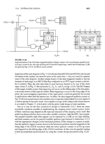
FIGURE 13.46
Implementation of the 4-bit data-triggered up/down binary counter with asynchronous parallel load,
(a) Logic circuit for the 7th stage showing the CO and BO output logic, where the NS functions Tj (H)
are given by Eqs. (12.5). (b) Block circuit symbol.
inspection of the state diagram in Fig. 13.42 indicates that DECDLYand INCDLY, the Up and
Dn inputs to the counter, can never be active at the same time — they are issued in separate
states of the state diagram. Another unique feature of this data-triggered counter is that the
memory of each stage is an FET D flip-flop configured as an FET toggle module (a divide-
by-2 counter). Thus, the only data input to each memory element is by way of the clock
input, where Tj in Fig. 13.46a represents T A,T B,T C, and T D in Eqs. (12.5). The FET feature
of the toggle module ensures that triggering will occur on the falling edge of the data pulse,
a necessary feature of this type of counter. Were triggering to occur on the rising edge of the
pulse, the nonoverlapping requirement of the input pulses could not generally be assured
in applications other than the present one. In effect, the data-triggered up/down counter in
Fig. 13.46 is an asynchronous state machine since it operates independent of a clock signal. It
is said to operate in the pulse mode. An in-depth coverage of this subject and related matters
is provided in Chapter 15, which deals with the pulse mode design of state machines.
Just as is true for the first system-level design in Subsection 13.6.1, there are many
acceptable variations possible in implementing the stepping motor control system. Some
of these variations may depend on the type and character of the stepping motor itself. But
aside from that possibility, there exists other suitable variations. Take the DPU, for example.
The parallel-loadable right shift register can be replaced by a USR set for right shifting,
and both counters can be the parallel loadable up/down type featured in Subsection 12.3.5
with the appropriate changes in the functional partition. If this change in counters is made,
then the up/down (upper) counter shown in the functional partition must be triggered on the
rising edge of the SYSCK waveform while the lower up/down counter is set for up count
and triggered on the falling edge of the SYSCK waveform. In this case the parallel loading
is best accomplished asynchronously by using the counter design presented in Fig. 12.28.