
Page 704 - Engineering Digital Design
P. 704
670 CHAPTER 13 / ALTERNATIVE SYNCHRONOUS FSM ARCHITECTURES
[21] Programmable Logic Data Book, Intel Corp., Santa Clara, CA, 1994.
[22] Programmable Logic Devices Data Handbook. Signetics Co., Sunnyvale, CA, 1992.
[23] The Programmable Logic Data Book. Xilinx, Inc., San Jose, CA, 1996.
[24] XACT, Logic Cell Array Macro Library. Xilinx, Inc., San Jose, CA, 1992.
Most texts in digital design do not attempt to cover digital design fundamentals together
with the organization and design of microprocessors (or microcontrollers) and computers.
Of those that do attempt this and for the reader who is interested in microprocessor and
computer design but who has had no previous experience in the field, the texts by Hayes
and Katz (both previously cited) and that by Shaw are given a qualified recommendation.
Usually the subject of computer organization and design is a challenge to develop in a single
dedicated text. So one might expect the treatment to be somewhat on the thin side in the
three texts cited above. Better sources for the beginning reader can be found in the text by
Mano and Kime, and in that by Pollard. In these last two references the reader will find
much more detailed information on computer organization and design. However, the reader
should expect to find only token coverage of digital design fundamentals in these texts.
[25] A. W. Shaw, Logic Circuit Design. Saunders College Publishing, Fort Worth, TX, 1991.
[26] M. M. Mano and C. R. Kime, Logic and Computer Design Fundamentals. Prentice-Hall, Engle-
wood Cliffs, NJ, 1997.
[27] L. H. Pollard, Computer Design andArchiteture. Prentice-Hall, Englewood Cliffs, NJ, 1990.
PROBLEMS
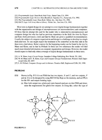
13.1 Shown in Fig. P13.1 is an FSM that has two inputs, X and 7, and two outputs, P
and Q. It is to be designed by using RET D flip-flops as the memory, and an FPLA
for the NS- and output-forming logic.
(a) Run both output race glitch and static hazard analyses on this FSM and deter-
mine the requirements for glitch-free outputs. In doing this, select the type of
CUT if Y
Pit if X
FIGURE P13.1