
Page 709 - Engineering Digital Design
P. 709
PROBLEMS 675
Sanity-
\ J ^ X \ \
ZitifX
x
' Vr^-^ x'' N — ^ V~^
V ^- — -^
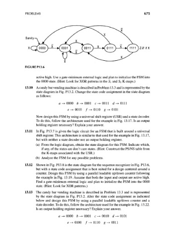
FIGURE P1 3.6
active high. Use a gate-minimum external logic and plan to initialize the FSM into
the 0000 state. (Hint: Look for XOR patterns in the Si and SQ K-maps.)
13.10 A candy bar vending machine is described in Problem 13.3 and is represented by the
state diagram in Fig. P13.2. Change the state code assignment in the state diagram
as follows:
0001 c->0011 d^
0101
Now design this FSM by using a universal shift register (USR) and a state decoder.
To do this, follow the architecture used for the example in Fig. 13.17. Is an output
holding register necessary? Explain your answer.
13.11 In Fig. P13.7 is given the logic circuit for an FSM that is built around a universal
shift register. This architecture is similar to that used for the example in Fig. 13.17,
but with neither a state decoder nor an output holding register.
(a) From the logic diagram, obtain the state diagram for this FSM. Indicate which,
if any, of the states are don't care states. (Hint: Construct the PS/NS table from
the K-maps associated with the USR.)
(b) Analyze the FSM for any possible problems.
13.12 Shown in Fig. P13.8 is the state diagram for the sequence recognizer in Fig. P13.6,
but with a state code assignment that is best suited for a design centered around a
counter. Design this FSM by using a parallel loadable up/down counter following
the example in Fig. 13.19. Assume that both the input and output are active high.
Find a gate-minimum external logic and plan to initialize the FSM into the 0000
state. (Hint: Look for XOR patterns.)
13.13 The candy bar vending machine is described in Problem 13.3 and is represented
by the state diagram in Fig. P13.2. Alter the state code assignment as indicated
below and design this FSM by using a parallel loadable up/down counter and a
state decoder. To do this, follow the architecture used for the example in Fig. 13.22.
Is an output holding register necessary? Explain your answer.
a -» 0000 b -> 0001 c -+ 0010 d -> 0101
e-+0100 /-»0110 g