
Page 710 - Engineering Digital Design
P. 710
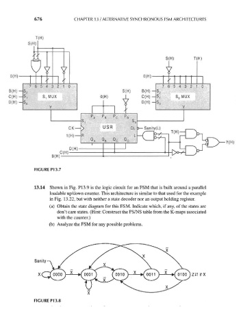
676              CHAPTER 13 / ALTERNATIVE SYNCHRONOUS FSM ARCHITECTURES


         C(H)-
         D(H)-


                                                                                                   Y(H)
                                                          I                        .  _   I *1 ^s
                                  D(H).
                              C(H)
                           B(H)
                    FIGURE P13.7


                    13.14 Shown in Fig. P13.9 is the logic circuit for an FSM that is built around a parallel
                          loadable up/down counter. This architecture is similar to that used for the example
                          in Fig. 13.22, but with neither a state decoder nor an output holding register.
                          (a) Obtain the state diagram for this FSM. Indicate which, if any, of the states are
                             don't care states. (Hint: Construct the PS/NS table from the K-maps associated
                             with the counter.)
                          (b) Analyze the FSM for any possible problems.


                    Sanity'
                           \ ^             ^    x                  \            \
                                                                                      ZiTifX
                                ' V^l^V' ^-^ ^S
                                         V ^—-^


                    FIGURE P13.8