
Page 713 - Engineering Digital Design
P. 713
PROBLEMS 679
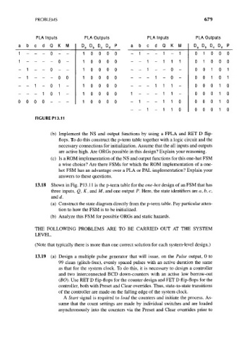
PLA Inputs PLA Outputs PLA Inputs PLA Outputs
a b c d Q K M D a D b D c D d P a b c d Q K M D a D b D c D d P
1 - - - 0 - - 1000 0 -1--1- 1 0100 0
•j _
_ _ _ 0 - 1000 0 - - 1 - 1 1 1 0100 0
- 1 _ - 0 - - 1000 0 _ _ 1 _ _ 0 - 0 0 1 0 1
- 1 - - - 0 0 1000 0 - - _ 1 - o - 0 0 1 0 1
- - 1 - 0 1 - 1000 0 - - - 1 1 1 - 0001 0
- - - 1 0 1 - 1000 0 1 - - - 1 1 - 0001 0
0 0 0 0 - - - 1000 0 - 1 - - 1 1 0 0001 0
- - 1 - 1 1 0 0001 0
FIGURE P13.11
(b) Implement the NS and output functions by using a FPLA and RET D flip-
flops. To do this construct the p-term table together with a logic circuit and the
necessary connections for initialization. Assume that the all inputs and outputs
are active high. Are ORGs possible in this design? Explain your reasoning.
(c) Is a ROM implementation of the NS and output functions for this one-hot FSM
a wise choice? Are there FSMs for which the ROM implementation of a one-
hot FSM has an advantage over a PLA or PAL implementation? Explain your
answers to these questions.
13.18 Shown in Fig. P13.11 is the p-term table for the one-hot design of an FSM that has
three inputs, Q, K, and M, and one output P. Here, the state identifiers are a, b, c,
and d.
(a) Construct the state diagram directly from the p-term table. Pay particular atten-
tion to how the FSM is to be initialized.
(b) Analyze this FSM for possible ORGs and static hazards.
THE FOLLOWING PROBLEMS ARE TO BE CARRIED OUT AT THE SYSTEM
LEVEL.
(Note that typically there is more than one correct solution for each system-level design.)
13.19 (a) Design a multiple pulse generator that will issue, on the Pulse output, 0 to
99 clean (glitch-free), evenly spaced pulses with an active duration the same
as that for the system clock. To do this, it is necessary to design a controller
and two interconnected BCD down-counters with an active low borrow-out
(BO). Use RET D flip-flops for the counter design and FET D flip-flops for the
controller, both with Preset and Clear overrides. Thus, state-to-state transitions
of the controller are made on the falling edge of the system clock.
A Start signal is required to load the counters and initiate the process. As-
sume that the count settings are made by individual switches and are loaded
asynchronously into the counters via the Preset and Clear overrides prior to