
Page 708 - Engineering Digital Design
P. 708
674 CHAPTER 13 / ALTERNATIVE SYNCHRONOUS FSM ARCHITECTURES
order, and assume that the activation levels for the inputs and outputs are
as follows:
For Fig. P13.4a—S(L) and T(H);X(H), Y(H) and Z(H)
For Fig. P13.4b — X(H) and Y(H); P(L) and Q(L)
Note that inverters cannot be used in dealing with an active low input or out-
put. For the FSM in Fig. P13.4b, make a clear distinction between the input
X and the irrelevant input symbol, X, used in the collapsed ROM program
table.
(2) Construct the logic circuit for the ROM implementation of each of these FSMs.
Use a block symbol for the ROM and assume the use of FET D flip-flops.
Consider that S and T are synchronous inputs and bounce-free. However, in
Fig. P13.4b both X and Y are asynchronous inputs, and input X arrives from
a mechanical switch. Thus, include any input or output conditioning circuits
that are necessary for a reliable glitch-free operation of the FSM. Initialize as
indicated in the state diagrams.
13.7 Construct the collapsed ROM program table for the FSM in Fig. PI 1.3. List the
present state, ABC, in ascending binary order. List any assumptions made.
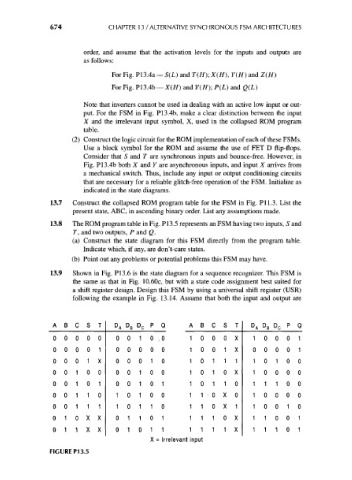
13.8 The ROM program table in Fig. P13.5 represents an FSM having two inputs, S and
T, and two outputs, P and Q.
(a) Construct the state diagram for this FSM directly from the program table.
Indicate which, if any, are don't-care states.
(b) Point out any problems or potential problems this FSM may have.
13.9 Shown in Fig. PI3.6 is the state diagram for a sequence recognizer. This FSM is
the same as that in Fig. 10.60c, but with a state code assignment best suited for
a shift register design. Design this FSM by using a universal shift register (USR)
following the example in Fig. 13.14. Assume that both the input and output are
A B C S T D A D B D c P Q A B C S T D A D B D c P Q
0000 0 0010, 0 1 0 0 0 X 1 0 0 0 1
0000 1 0000 0 1 0 0 1 X 0000 1
0 0 0 1 X 0001 0 1 0 1 1 1 1 0 1 0 0
0010 0 0010 0 1 0 1 0 X 1000 0
0 0 1 0 1 0 0 1 0 1 1 0 1 1 0 1 1 1 0 0
0 0 1 1 0 1 0 1 0 0 1 1 - 0 X 0 1000 0
0 0 1 1 1 1 0 1 1 0 1 1 0 X 1 1 0 0 1 0
0 1 0 X X 0 1 1 0 1 1 1 1 0 X 1 1 0 0 1
0 1 1 X X 0 1 0 1 1 1 1 1 1 X 1 1 1 0 1
X = Irrelevant input
FIGURE P13.5