
Page 701 - Engineering Digital Design
P. 701
13.7 DEALING WITH UNUSUALLY LARGE CONTROLLER 667
'
Input
Conditioning i^L> Output
/|px Circuits NS^ PS ^ PLD iVMife V*"" /
r/Mitc
NS PLD Memory ••
-*>
PS Feedback
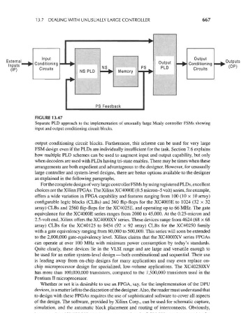
FIGURE 13.47
Separate PLD approach to the implementation of unusually large Mealy controller FSMs showing
input and output conditioning circuit blocks.
output conditioning circuit blocks. Furthermore, this scheme can be used for very large
FSM design even if the PLDs are individually insufficient for the task. Section 7.6 explains
how multiple PLD schemes can be used to augment input and output capability, but only
when decoders are used with PLDs having tri-state enables. There may be times when these
arrangements are both expedient and advantageous to the designer. However, for unusually
large controller and system-level designs, there are better options available to the designer
as explained in the following paragraphs.
For the complete design of very large controller FSMs by using registered PLDs, excellent
choices are the Xilinx FPGAs. The Xilinx XC4000E (0.5 micron-5 volt) series, for example,
offers a wide variation in FPGA capability and features ranging from 100(10x 10 array)
configurable logic blocks (CLBs) and 360 flip-flops for the XC4003E to 1024 (32 x 32
array) CLBs and 2560 flip-flops for the XC4025E, and operating up to 66 MHz. The gate
equivalence for the XC4000E series ranges from 2000 to 45,000. At the 0.25-micron and
2.5-volt end, Xilinx offers the XC4000XV series. These devices range from 4624 (68 x 68
array) CLBs for the XC40125 to 8454 (92 x 92 array) CLBs for the XC40250 family
with a gate equivalency ranging from 80,000 to 500,000. This series will soon be extended
to the 2,000,000 gate-equivalency level. Xilinx claims that the XC4000XV series FPGAs
can operate at over 100 MHz with minimum power consumption by today's standards.
Quite clearly, these devices lie in the VLSI range and are large and versatile enough to
be used for an entire system-level design—both combinational and sequential. Their use
is leading away from on-chip designs for many applications and may even replace on-
chip microprocessor design for specialized, low-volume applications. The XC40250XV
has more than 100,000,000 transistors, compared to the 7,500,000 transistors used in the
Pentium II microprocessor.
Whether or not it is desirable to use an FPGA, say, for the implementation of the DPU
devices, is a matter left to the discretion of the designer. Also, the reader must understand that
to design with these FPGAs requires the use of sophisticated software to cover all aspects
of the design. The software, provided by Xilinx Corp., can be used for schematic capture,
simulation, and the automatic block placement and routing of interconnects. Obviously,