
Page 740 - Engineering Digital Design
P. 740
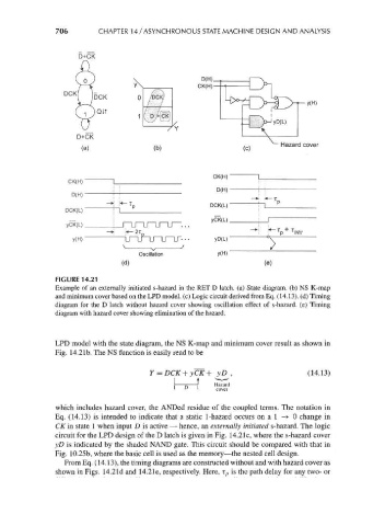
706         CHAPTER 14/ASYNCHRONOUS STATE MACHINE DESIGN AND ANALYSIS


                           D+CK


                                                           D(H)
                                                          CK(H)


                                                                               Hazard cover


                            _       ,                         CK(H)
                        CK(H)       [_ _
                            _ M _                              D(H)
                         D,H, - - -

                       DCK,U, - -T _


                                  -»j  *-2T D        '"
                         y(H)          Lrorrnj LT- • •        ycxu
                                          Oscillation          y(H)
                                      (d)                                  (e)
                    FIGURE 14.21
                    Example of an externally initiated s-hazard in the RET D latch, (a) State diagram, (b) NS K-map
                    and minimum cover based on the LPD model, (c) Logic circuit derived from Eq. (14.13). (d) Timing
                    diagram for the D latch without hazard cover showing oscillation effect of s-hazard. (e) Timing
                    diagram with hazard cover showing elimination of the hazard.


                    LPD model with the state diagram, the NS K-map and minimum cover result as shown in
                    Fig. 14.21b. The NS function is easily read to be


                                             Y = DCK+yCK + yD ,                       (14.13)
                                                              Hazard
                                                   1  D  1 l
                                                     "        cover
                    which includes hazard cover, the ANDed residue of the coupled terms. The notation in
                    Eq. (14.13) is intended to indicate that a static 1-hazard occurs on a 1 -> 0 change in
                    CK in state 1 when input D is active — hence, an externally initiated s-hazard. The logic
                    circuit for the LPD design of the D latch is given in Fig. 14.21c, where the s-hazard cover
                    yD is indicated by the shaded NAND gate. This circuit should be compared with that in
                    Fig. 10.25b, where the basic cell is used as the memory—the nested cell design.
                       From Eq. (14.13), the timing diagrams are constructed without and with hazard cover as
                    shown in Figs. 14.21d and 14.21e, respectively. Here, r p is the path delay for any two- or