
Page 741 - Engineering Digital Design
P. 741
14.10 DETECTION AND ELIMINATION OF TIMING DEFECTS 707
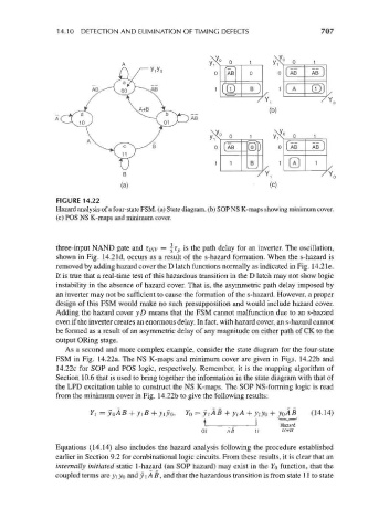
FIGURE 14.22
Hazard analysis of a four-state FSM. (a) State diagram, (b) SOP NS K-maps showing minimum cover.
(c) POS NS K-maps and minimum cover.
three-input NAND gate and T ]NV = f T P is the path delay for an inverter. The oscillation,
shown in Fig. 14.2 Id, occurs as a result of the s-hazard formation. When the s-hazard is
removed by adding hazard cover the D latch functions normally as indicated in Fig. 14.21e.
It is true that a real-time test of this hazardous transition in the D latch may not show logic
instability in the absence of hazard cover. That is, the asymmetric path delay imposed by
an inverter may not be sufficient to cause the formation of the s-hazard. However, a proper
design of this FSM would make no such presupposition and would include hazard cover.
Adding the hazard cover yD means that the FSM cannot malfunction due to an s-hazard
even if the inverter creates an enormous delay. In fact, with hazard cover, an s-hazard cannot
be formed as a result of an asymmetric delay of any magnitude on either path of CK to the
output ORing stage.
As a second and more complex example, consider the state diagram for the four-state
FSM in Fig. 14.22a. The NS K-maps and minimum cover are given in Figs. 14.22b and
14.22c for SOP and POS logic, respectively. Remember, it is the mapping algorithm of
Section 10.6 that is used to bring together the information in the state diagram with that of
the LPD excitation table to construct the NS K-maps. The SOP NS-forming logic is read
from the minimum cover in Fig. 14.22b to give the following results:
Y 0 = y\AB + y,A + yiy 0 + y 0AB (14.14)
Equations (14.14) also includes the hazard analysis following the procedure established
earlier in Section 9.2 for combinational logic circuits. From these results, it is clear that an
internally initiated static 1 -hazard (an SOP hazard) may exist in the YQ function, that the
coupled terms are y\ jo and y \ A B , and that the hazardous transition is from state 1 1 to state