
Page 742 - Engineering Digital Design
P. 742
708 CHAPTER 14/ASYNCHRONOUS STATE MACHINE DESIGN AND ANALYSIS
y,(H)
Inverter
causing
s-hazard
Fictitious LPD
memory elements
•y 0(H)
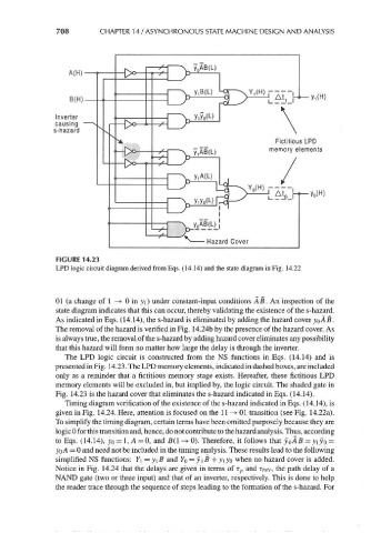
FIGURE 14.23
LPD logic circuit diagram derived from Eqs. (14.14) and the state diagram in Fig. 14.22
01 (a change of 1 —> 0 in ji) under constant-input conditions AB. An inspection of the
state diagram indicates that this can occur, thereby validating the existence of the s-hazard.
As indicated in Eqs. (14.14), the s-hazard is eliminated by adding the hazard cover yoAB.
The removal of the hazard is verified in Fig. 14.24b by the presence of the hazard cover. As
is always true, the removal of the s-hazard by adding hazard cover eliminates any possibility
that this hazard will form no matter how large the delay is through the inverter.
The LPD logic circuit is constructed from the NS functions in Eqs. (14.14) and is
presented in Fig. 14.23. The LPD memory elements, indicated in dashed boxes, are included
only as a reminder that a fictitious memory stage exists. Hereafter, these fictitious LPD
memory elements will be excluded in, but implied by, the logic circuit. The shaded gate in
Fig. 14.23 is the hazard cover that eliminates the s-hazard indicated in Eqs. (14.14).
Timing diagram verification of the existence of the s-hazard indicated in Eqs. (14.14), is
given in Fig. 14.24. Here, attention is focused on the 11 —>• 01 transition (see Fig. 14.22a).
To simplify the timing diagram, certain terms have been omitted purposely because they are
logic 0 for this transition and, hence, do not contribute to the hazard analysis. Thus, according
to Eqs. (14.14), j 0 = 1, A = 0, and B(\ -* 0). Therefore, it follows that y 0AB = y }y 0 =
y Q A = 0 and need not be included in the timing analysis. These results lead to the following
simplified NS functions: Y\ =y\B and 7o = y \B + y\y$ when no hazard cover is added.
Notice in Fig. 14.24 that the delays are given in terms of T P and T INV, the path delay of a
NAND gate (two or three input) and that of an inverter, respectively. This is done to help
the reader trace through the sequence of steps leading to the formation of the s-hazard. For