
Page 743 - Engineering Digital Design
P. 743
14.10 DETECTION AND ELIMINATION OF TIMING DEFECTS 709
A(H) A(H)
B(H) | . B(H)
y,(H) ; L y t(H)
Static
1 -hazard
y,B(L)
y, AB(L) i I y, B(L)
yiy (L) ~~^ ViVoC-)
0
+T £
INV
y 0AB(L) _
(b)
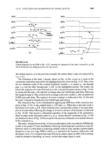
FIGURE 14.24
Timing diagrams for the FSM in Fig. 14.23, showing (a) formation of the static 1-hazard in yo and
(b) its elimination by adding hazard cover (see arrow).
this timing analysis, as in the previous example, the relative delay values are expressed by
The formation of the static 1 -hazard, shown in Fig. 14.24a, occurs as a result of the
asymmetric path delay imposed by the highlighted inverter shown in Fig. 14.23. Thus, there
are two alternative paths of the coupled (feedback) variable y\ to output yo: one through
gate y\ yo and the other through gate y \ A B via the highlighted inverter. The reader can
follow the sequence of events that lead up to this s-hazard formation shown in Fig. 14.24a
by noting that the term y i B is the first to change after one NAND gate path delay following
the change in input B. This is followed by a change in the state variable y\ after an additional
NAND gate path delay. The sequence of events continues as indicated in Fig. 14.24a until
the static 1 -hazard is formed after four NAND gate path delays.
The s-hazard in Fig. 14.24 is eliminated by applying the SOP form of the consensus law,
given in Eqs. (3.14), to the coupled terms y\AB and yiyo- When this is done the result is
the hazard cover term yoAB, which eliminates the s-hazard after a delay of one gate delay
plus an inverter delay following the change in B well in advance of the hazard, as indicated
in Fig. 14.24b. This hazard is eliminated regardless of the magnitude of the asymmetric
delay on either of the alternative paths of y\ to yo. Notice that the waveforms in Fig. 14.24b
are identical to those of Fig. 14.24a except for the presence of hazard cover and the absence
of the s-hazard in y 0.
The static 1 -hazard shown in Fig. 14.24a is nondisruptive in the sense that the FSM finally
resides in the proper 01 state immediately following a brief improper transition to state 00.
However, there is a short delay in achieving stability in the 01 state, and this could be highly
disruptive to any next-stage FSM to which yo is attached if the hazard is sufficiently well
developed. Also, if it is required that state 00 issue an output signal, an ORG will result that
could be disruptive depending, of course, on how that output signal is used.