
Page 144 - Industrial Power Engineering and Applications Handbook
P. 144
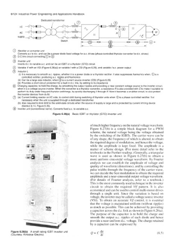
6/124  Industrial Power Engineering and Applications  Handbook
                         Dedicated transformer

             AC  47"
                   I
            supply 4% 3


            Rectifier or converter unit
            Converts a.c to d.c.  and can be a  ower diode fixed voltage for a.c. drives (phase controlled thyristor converter for d.c. drives)
            D.C.link circuit connectingat06
            Inverter unit
            Inverts d.c. to variable a.c. and can be an IGBT or a thyristor (GTO) circuit.
            Variable Vwith an VSI (Figure 6.28(a)) or variable I with a CSI (Figure 6.29), and variable fax. power output
            Inductor L
            (i) It is necessary to smooth a.c. ripples, whether it is a power diode or a thyristor rectifier. It also suppresses harmonics when, @is a
              controlled rectifier, producing a.c.  rip  les and harmonics
            (ii) Can be a large size inductor, when 6 is a current source inverter (CSI) (Figure 6.29)
            (iii) Provides a short-circuit protection for a fault in d.c. link, by adding to its impedance
            Charging capacitor, to hold the charge, by smoothing the output ripples and providing a near constant voltage source to the inverter circuit,
            when it is a voltage source inverter. When the converter is a thyristor converter, a resistance R is also provided with C to make it suitable to
            perform its duty under frequent thyristor switchings, by quickly discharging it through R. Now it becomes a snubber circuit, to also protect
            the inverter devices from duldt.
            (a) Current limiting reactor on I/C side, to control dildtduring switching of thyristor units when @is a phase controlled rectifier. Not
              necessary when the unit is supplied through a dedicated transformer.
            (b) Also required  to limit dildt to the solid-state circuits when the source of supply is large and is protected by current limiting device
              (Section 6.14, Figure 6.35).
            Inverter unit (conventional name). Converts fixed ax. to variable ax.
                                Figure 6.26(a)  Basic IGBT or thyristor (GTO) inverter unit


                                                      of much higher frequency on the natural voltage waveform.
                                                      Figure  6.27(b)  is  a  simple block  diagram  for a  PWM
                                                      scheme, the natural voltage being the voltage obtained
                                                      by the switching of the IGBTs. The carrier wave can be
                                                      of any shape, the frequency of which is altered, to obtain
                                                      the required degree of modulation, and hence the voltage,
                                                      while  the  amplitude  is kept  fixed.  The  amplitude  is  a
                                                      matter  of  scheme design.  (For more detail refer  to the
                                                      textbooks in the Further reading.) Generally, a triangular
                                                      wave  is used  as  shown  in  Figure  6.27(b)  to  obtain  a
                                                      more uniform sinusoidal voltage waveform. By Fourier
                                                      analysis we can establish  the amplitude of  voltage and
                                                      quality of waveform (distortions), and by controlling the
                                                      pulse widths through the frequency of the carrier wave,
                                                      we can decide the best modulation to obtain the required
                                                      amplitude and a near-sinusoidal output voltage waveform.
                                                      (For  details  of  Fourier  analysis,  refer  to  a  textbook.)
                                                      This is the most commonly used technique in the inverter
                                                      circuit  to  obtain  the  required  Vlf  pattern.  It  is  also
                                                      economical and can be used to control multi-motor drives
                                                      through  a  single  unit.  Since the  variation  is  based  on
                                                      voltage, the inverter may be called a voltage source inverter
                                                      (VSI). To obtain  an accurate  Vlfcontrol,  it is essential
                                                      that the voltage is maintained uniform (without ripples)
                                                      as much as possible. This can be achieved by providing
                                                      a capacitor across the d.c. link as shown in Figure 6.26(a).
                                                      The purpose  of  the capacitor is to hold the charge and
                                                      smooth the output a.c. ripples of  each diode and hence
                                                      provide a near-uniform d.c. voltage. The charge retained
                                                      by a capacitor can be expressed by
                                                            du
        Figure 6.26(b)  A small rating IGBT inverter unit   Q=C-
        (Courtesy: Kirloskar  Electric)                     dt