
Page 145 - Industrial Power Engineering and Applications Handbook
P. 145
Static controls and braking of motors 61125
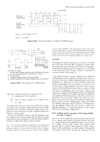
Pulse widths
AC output
voltage pulses
AC input
instantaneous
voltage
waveform
C D ztl+fP+t3+t4+t5ft6
~
r
and V,,, = V,iC I
D F
Figure 6.27(a) Varying the output a c voltage with PWM technique
ai wcll as the suitability of the mechanical sy\tein must he pre-
checked. When. however, such a situation be desirable. the frequency
may be varied to the desired lebel by twitching. kccping the output
voltage to the rated value. Since the torque of the motor will now
f reduce a IIN, this must be checked with the load requirement.
In GTOs
* The frequency in the inverter circuit is varied by switching
the GTO pairs ON and OFF repeatedly through their
I
Firing
Modulator circuit gate control in each one half cycle. The rate of frequency
variation will depend upon the frequency of switching
@) Reference voltage of the GTO pairs. The voltage variation is obtained by
Inverter natural voltage waveform before modulation improved varying the gate firing angle, a.
to a near sinusoidal waveform, with the use of Land C
@ Carrier voltage By using converter-inverter combinations in different
Triangular voltage waveform of fixed amplitude
@ Variable frequency and modulated voltage output (Vif ) as desired configurations and by applying a proper gate control. a
variety of fixed and variable output parameters of a fixed
parameter a.c. input power can be obtained. When the
Figure 6.27(b) Block diagram for a PWM scheme
motor is operating at very low speeds, say, below 5% of
N,, the motor voltage demand is also low. If the inverter
circuit is load commutated (motor side), its phase current
will have to commutate with a very low voltage at the
load side. It is difficult to guarantee reliable commutation
where Q = charge stored by the capacitor unit at such low voltages. Pulse width commutation is therefore
C = capacitance of the capacitor also employed in thyristor drives when the motor has to
du operate at very low speeds. Where the motors are very
- rate of voltage change or a.c. ripples in the large, cyclo converters can also be employed. Below we
=
dt discuss a few inverter configurations. Generally PWM
d.c. link
(for IGBTs) and gate control schemes (for thyristors)
The higher the value of C, the lower will be the voltage may be applied to these inverter circuits to obtain the
overshoots in the rectified voltage and the inverter circuit required variable a.c. supply parameters at the output
would be fed by an almost constant voltage source. The line to suit a particular requirement.
capacitor in the circuit also provides an indirect protection
from the voltage surges. 6.9.3 Voltage source inverter (VSI) using IGBTs
The above method is used to vary the frequency and (to vary V andf)
the voltage ot the inverter output (motor side) according
to the process needs, irrespective of the electronics scheme This is the most commonly used inverter for the control
adopted to obtain the required speed control. of a.c. motors and is shown in Figure 6.28(a). The fixed
d.c. voltage from the uncontrolled rectifier converter acts
as a voltage source to the inverter. The voltage in the
,Vrur The variation of frequency is generally up to its fundamental
value. ].e. 0-50 or 0-60 Hr. in vicw of the fact that the motor is inverter unit is varied to the required level by using a
generally required to operate below the base speed. At higher pulse width modulation, as noted earlier. Through the
frecpencie\ the motor \n ill overspeed. for v hich its own suitab~lity switching circuit of the inverter the frequency of the