
Page 462 - Instrumentation Reference Book 3E
P. 462
Digital voltmeters and digital multirneters 445
or a 0. This process is repeated for each bit of the If tl corresponds to a fixed number of counts, nl ,
DAC. The conversion period for the successive- of a clock having a period r and tl is measured
approximation ADC technique is fixed for a with the same clock, say, 172 counts, then
given ADC irrespective of the signal level and is
1: 'in
equal to N,. where N is the number of bits and 7 n2=-.n 1
is the cycle time for determining a single bit. Vref
Integrated circuit successive-approximation The values of the R and C components of the
logic-generating chips are available to be used in integrator do not appear in the defining equation
conjunction with standard DACs and compara- of the ADC; neither does the frequency of the
tors to produce medium-speed ADCs. A typical reference clock. The only variable which appears
8-bit ADC will have a conversion time of lops. explicitly in the defining equation is the reference
Successive-approximation ADCs are limited to 16 voltage. The effect of the offset voltage on the
bits, equivalent to a five-decade conversion. comparator will be minimized as long as its value
remains constant over the cycle and also provid-
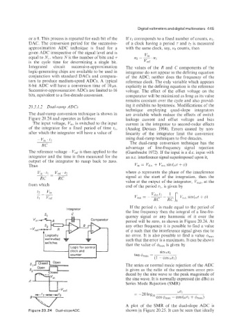
20.3.1.2 Dual-ramp ADCs ing it exhibits no hysteresis. Modifications of the
technique employing quad-slope integrators
The dual-ramp conversion technique is shown in are available which reduce the effects of switch
Figure 20.24 and operates as follows: leakage current and offset voltage and bias
The input voltage, V,,. is switched to the input current in the integrator to second-order effects
of the integrator for a fixed period of time tl, (Analog Devices 1984). Errors caused by non-
after which the integrator will have a value of linearity of the integrator limit the conversion
using dual-ramp techniques to five decades.
vi, ' t 1
~ The dual-ramp conversion technique has the
RC advantage of line-frequency signal rejection
The reference voltage - Vref is then applied to the (Gumbrecht 1972). If the input is a d.c. input with
integrator and the time is then measured for the an a.c. interference signal superimposed upon it,
output of the integrator to ramp back to zero.
Thus V,, = Vd + V, c. sin (ut + 6)
where d represents the phase of the interference
v,, . ti - Vreref . t2
-
~- ~ signal at the start of the integration, then the
RC RC value at the output of the integrator, Vnut+ at the
from which end of the period tl, is given by
tr vin
-
-~
-
tl Vref
If the period fl is made equal to the period of
Integrator
the line frequency then the integral of a line-fre-
quency signal or any harmonic of it over the
Vi n period will be zero, as shown in Figure 20.24. At
any other frequency it is possible to find a value
-"ref of 4 such that the interference signal gives rise to
no error. It is also possible to find a value Omax
such that the error is a maximum. It can be shown
that the value of 4,,, is given by
sin wtl
tand,,, =
(1 - C0Scc;tl)
The series or normal mo6e rejection of the ADC
is given as the ratio of the maximum error pro-
duced by the sine wave to the peak magnitude of
the sine wave. It is normally expressed (in dBs) as
Series Mode Rejection (SMR)
wt 1
= -20 loglo
cos d,,, - cos (Wfl + 4,,,)
A plot of the SMR of the dual-slope ADC is
Figure 20.24 Dual-slopeADC. shown in Figure 20.25. It can be seen that ideally